Pixel driving circuit, pixel driving method, array substrate and display device

A technology of a pixel driving circuit and a driving unit, applied in the field of pixel driving circuits and methods, array substrates and display devices, capable of solving problems such as uneven brightness and affecting image display effects, and achieving the same brightness and good display effects

Active Publication Date: 2015-08-19
BOE TECH GRP CO LTD
View PDF7 Cites 27 Cited by
  • Summary
  • Abstract
  • Description
  • Claims
  • Application Information

AI Technical Summary

Problems solved by technology

[0004] In order to solve the problem of uneven brightness of AMOLED in the prior art and affecting the display effect of the entire image, an embodiment of the present invention provides a pixel driving circuit and method, an array substrate and a display device

Method used


Image

  • Pixel driving circuit, pixel driving method, array substrate and display device
  • Pixel driving circuit, pixel driving method, array substrate and display device
  • Pixel driving circuit, pixel driving method, array substrate and display device

Examples


Embodiment Construction

[0048] In order to make the object, technical solution and advantages of the present invention clearer, the implementation manner of the present invention will be further described in detail below in conjunction with the accompanying drawings.

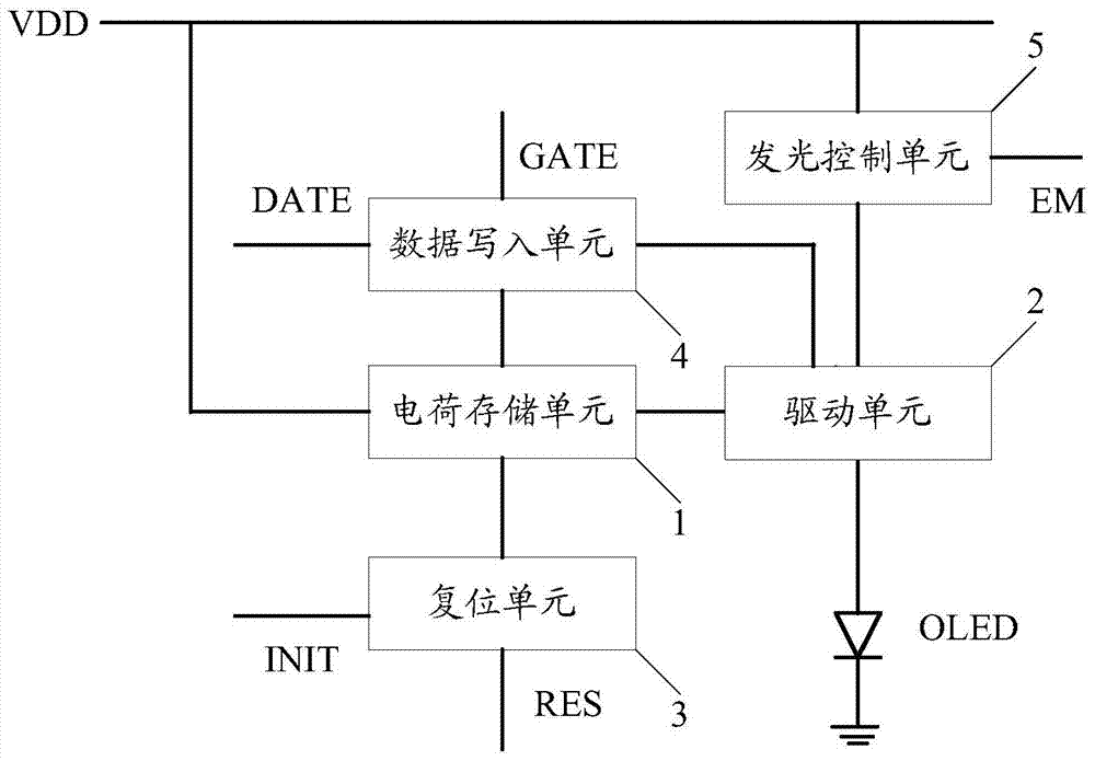
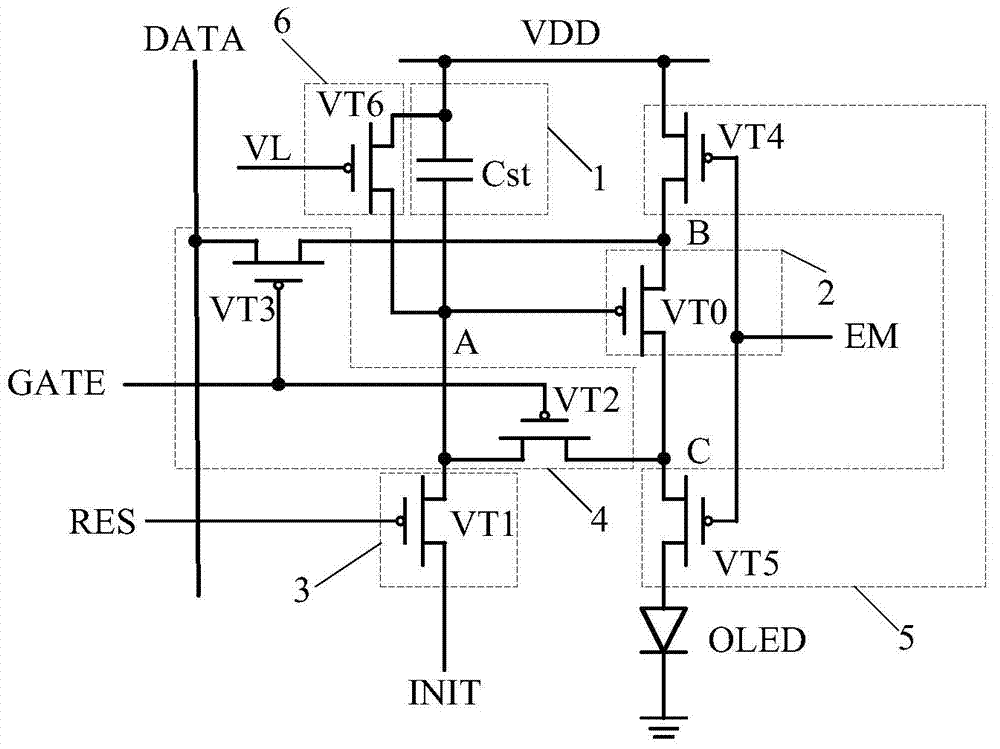
[0049] An embodiment of the present invention provides a pixel driving circuit for driving an organic light emitting diode to emit light, see figure 1 , the pixel driver circuit includes:

[0050] A charge storage unit 1, the first terminal of the charge storage unit 1 is connected to a power supply voltage signal;

[0051] The drive unit 2, the control terminal of the drive unit 2 is connected to the second terminal of the charge storage unit 1, and is used to generate a drive for driving the organic light emitting diode (OLED) to emit light when the voltage at the second terminal of the charge storage unit 1 is greater than the threshold voltage of the drive unit 1 current;

[0052] The reset unit 3 is connected to the second end of ...


PUM


Abstract

The invention discloses a pixel compensation circuit, an array substrate and a display device, and belongs to the technical field of semiconductors. The pixel compensation circuit comprises a charge storage unit of which a first end is connected to a power supply voltage signal, a driving unit of which the control end is connected with a second end of the charge storage unit and which is used for generating driving current for driving an OLED to emit light when the voltage at the second end of the charge storage unit is greater than the threshold voltage of the driving unit, a reset unit which is connected with the second end of the charge storage unit and used for writing the voltage of an initial voltage signal into the second end of the charge storage unit in the reset stage, a data writing unit which is connected with the second end of the charge storage unit and used for writing the voltage of a data voltage signal and the threshold voltage of the driving unit into the second end of the charge storage unit in the data writing stage, and a light emitting control unit which is connected with the driving unit and used for making the power supply voltage signal written into the driving unit to generate driving current in the light emitting control stage. Correct data writing is ensured.

Description

technical field [0001] The present invention relates to the technical field of semiconductors, in particular to a pixel driving circuit and method, an array substrate and a display device. Background technique [0002] Active Matrix Organic Light Emitting Diode (AMOLED) display is a display technology used in TVs and mobile devices. It is sensitive to power consumption due to its low power consumption, low cost, and large size. It has broad application prospects in portable electronic devices. [0003] The organic light emitting diode (Organic Light Emitting Diode, referred to as OLED) in AMOLED can emit light and is driven by the driving current generated by the thin film transistor (Thin Film Transistor, referred to as TFT), but as time changes, the threshold voltage of TFT may change , resulting in the input of the same voltage to the TFT, the driving current generated by the TFT is inconsistent, which leads to different brightness of each OLED, and the uneven brightness...

Claims


Application Information

Patent Timeline
Patent Type & Authority Applications(China)
IPC IPC(8): G09G3/32
CPCG09G3/3233G09G2300/0819G09G2300/0861G09G2310/0251G09G2310/0262G09G2320/043G09G3/3258G09G2300/0426G09G2320/0214G09G2320/0233G09G2320/0626G09G2330/023
Inventor 段立业王俪蓉李重君钟杰兴林俊杰
Owner BOE TECH GRP CO LTD
Why Eureka
Try Eureka