Wafer buffering apparatus in semiconductor device

An in-equipment, semiconductor technology, used in semiconductor/solid-state device manufacturing, transportation and packaging, conveyor objects, etc., can solve problems such as increasing the burden on the robot, increasing the number of positions for the robot to pick up and deliver wafers, and affecting the process time. The effect of shortening the time required for the process, improving the work efficiency and being easy to use

Active Publication Date: 2016-02-10
SHENYANG KINGSEMI CO LTD
View PDF6 Cites 9 Cited by
  • Summary
  • Abstract
  • Description
  • Claims
  • Application Information

AI Technical Summary

Problems solved by technology

In the prior art, there are generally two wafer cassettes for wafer buffering in devices with similar functions. The position of the wafer cassettes is fixed, or fixed on the same plane according to a set angle, or arranged up and down, so that This increases the number of stations for the manipulator to pick up and deliver wafers, which not only increases the burden on the manipulator, but also affects the process time

Method used


Image

  • Wafer buffering apparatus in semiconductor device
  • Wafer buffering apparatus in semiconductor device
  • Wafer buffering apparatus in semiconductor device

Examples


Embodiment Construction

[0028] The present invention will be described in further detail below in conjunction with the accompanying drawings.

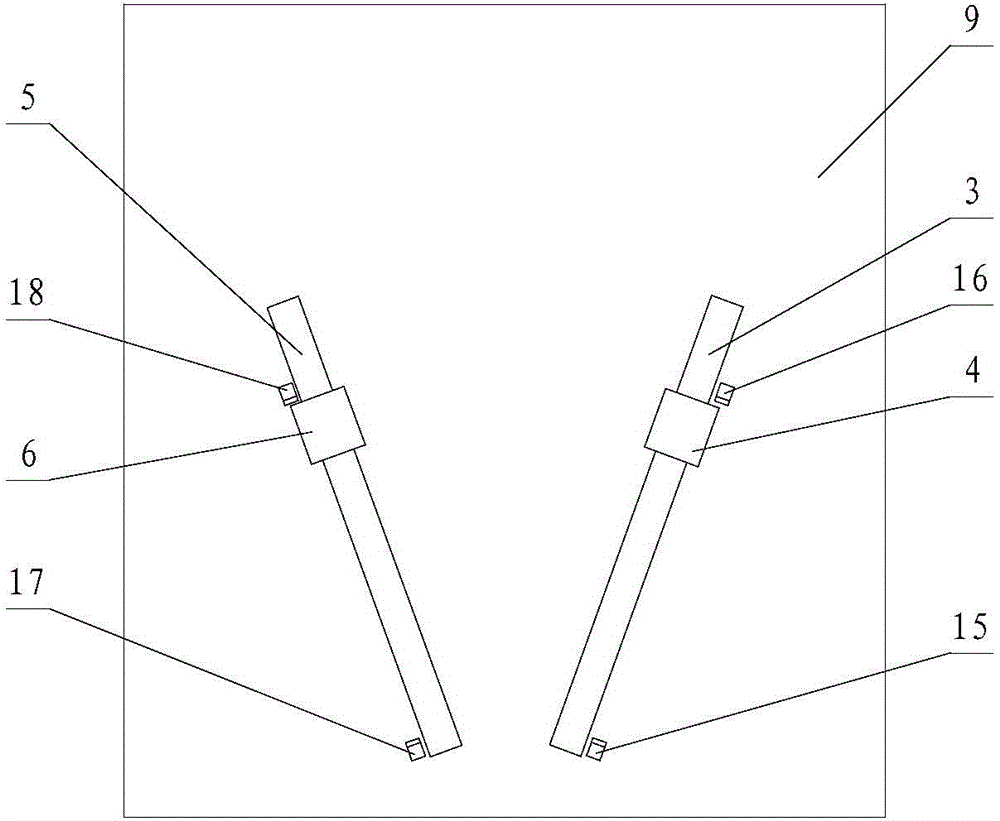
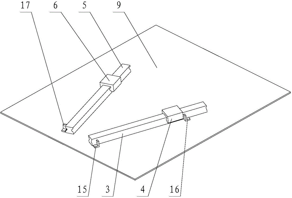
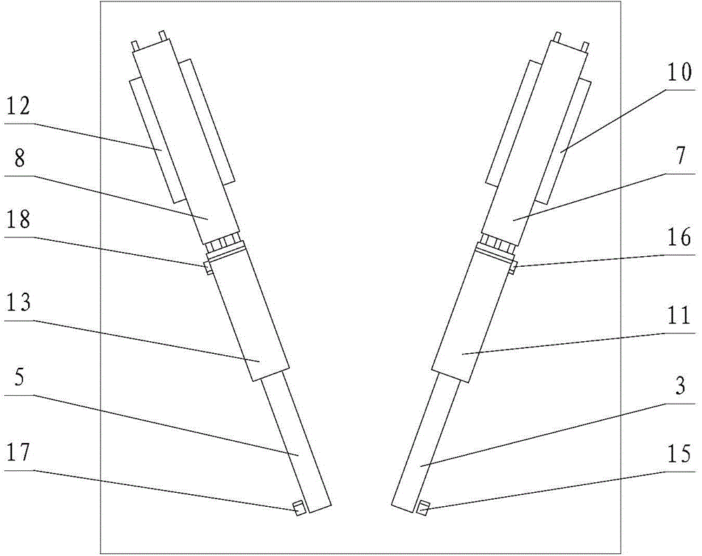
[0029] Such as Figure 1~6 As shown, the present invention includes a first wafer box 1, a second wafer box 2, a first linear guide 3, a first slider 4, a second linear guide 5, a second slider 6, a first cylinder 7, The second cylinder 8, the bottom plate 9, the sensor 14, the first sensor scanning baffle 20 and the second sensor scanning baffle 21, wherein the bottom plate 9 is the motion platform of the entire wafer buffer device, and can be fixed inside the semiconductor equipment according to the actual situation .

[0030] The cylinder body of the first cylinder 7 is fixed on the base plate 9 by the first fixed plate 10, and the cylinder body of the second cylinder 8 is fixed on the base plate 9 by the second fixed plate 12. 9, the first linear guide 3 on the second cylinder 8 is provided with a second linear guide 5 fixed on the base plate 9 in the o...


PUM


Abstract

The present invention belongs to the field of wafer processing in the semiconductor industry, and specifically a wafer buffering apparatus in a semiconductor device. The wafer buffering apparatus in the semiconductor device includes a first wafer box, a second wafer box, a first air cylinder, a second air cylinder and a bottom plate. The first air cylinder and the second air cylinder are mounted on the bottom plate separately. The first wafer box and the second wafer box are connected with input ends of the first air cylinder and the second air cylinder respectively, and are driven by the first air cylinder and the second air cylinder respectively to alternately move to the position that a manipulator picks up and delivers wafers, namely, the first wafer box or the second wafer box move to the position that the manipulator picks up and delivers wafers, and the second wafer box or the first wafer box locate on a vacancy position. The wafer buffering apparatus in the semiconductor device has simple structure, is convenient to operate. A plurality of wafer boxes provide the function that the manipulator picks up and delivers wafers at the same position through a linear guide way so as to ease the burden of the manipulator, reduce the defect of movement time increasing of the manipulator due to more positions, shorten the time required by processing, and improve the working efficiency.

Description

technical field [0001] The invention belongs to the field of wafer processing in the semiconductor industry, in particular to a wafer buffering device used in semiconductor equipment. Background technique [0002] The processing of wafers in the semiconductor industry needs to go through different process units or even different equipment. Among them, the manipulator undertakes the task of wafer transfer. If the time spent on wafer processing is different and there are differences in speed, then it cannot be transferred directly. Generally, it needs An intermediate link to buffer and transfer wafers. In the prior art, there are generally two wafer cassettes for wafer buffering in devices with similar functions. The position of the wafer cassettes is fixed, or fixed on the same plane according to a set angle, or arranged up and down, so that This increases the number of stations for the manipulator to pick up and deliver wafers, which not only increases the burden on the man...

Claims


Application Information

Patent Timeline
Patent Type & Authority Applications(China)
IPC IPC(8): H01L21/673H01L21/677H01L21/67
Inventor 张爽王继周门恩国
Owner SHENYANG KINGSEMI CO LTD
Why Eureka
Try Eureka