Thin-film transistor array substrate, display panel and display device

A thin-film transistor and array substrate technology, which is applied in the field of display panels and display devices, can solve the problems of low pixel aperture ratio and large area occupied by scanning lines, and achieve uniform color mixing, excellent display quality effects, and increased area effects

Inactive Publication Date: 2016-04-13
KUSN INFOVISION OPTOELECTRONICS
View PDF5 Cites 10 Cited by
  • Summary
  • Abstract
  • Description
  • Claims
  • Application Information

AI Technical Summary

Problems solved by technology

[0006] The object of the present invention is to provide a thin-film transistor array substrate, and a display panel and a display device having the thin-film transistor array substrate, so as to solve the problem that the scanning line occupies a large area and the pixel opening is large in the double-scanning line pixel array structure of the existing array substrate. low rate problem

Method used


Image

  • Thin-film transistor array substrate, display panel and display device
  • Thin-film transistor array substrate, display panel and display device
  • Thin-film transistor array substrate, display panel and display device

Examples


Embodiment Construction

[0022] In order to further explain the technical means and effects of the present invention to achieve the intended purpose of the invention, the specific implementation, structure, features and effects of the present invention will be described in detail below in conjunction with the accompanying drawings and examples.

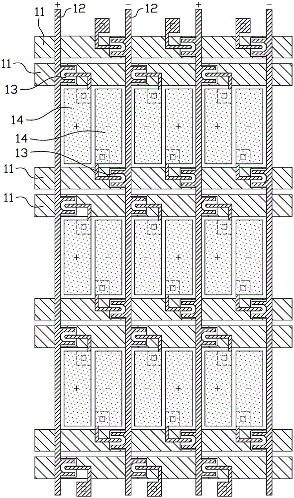
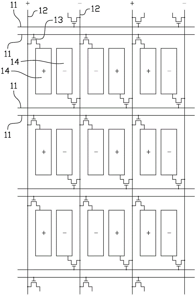
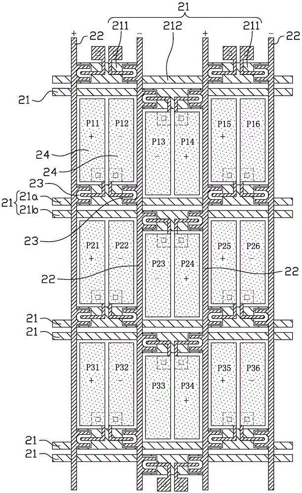
[0023] image 3 is a schematic plan view of a thin film transistor array substrate in an embodiment of the present invention, Figure 4 for image 3 The equivalent circuit diagram of the TFT array substrate, Figure 5 It is a partial cross-sectional schematic diagram of a thin film transistor array substrate in an embodiment of the present invention, please refer to Figure 3 to Figure 5 , the thin film transistor array substrate has a dual scanning line pixel array structure, the thin film transistor array substrate includes a base substrate 20 and a plurality of scanning lines 21, a plurality of data lines 22, a plurality of TFTs 23 and a plurality of Ea...


PUM


Abstract

The invention provides a thin-film transistor array substrate. The thin-film transistor array substrate comprises a plurality of scanning lines, a plurality of data lines, a plurality of TFTs and a plurality of pixel electrodes, which are arranged on a substrate, wherein each pixel electrode is connected with the corresponding scanning line and data line through the corresponding TFT; the thin-film transistor array substrate has a double-scanning line pixel array structure; the plurality of data lines divide each scanning line in the plurality of scanning lines into a plurality of first scanning segments and a plurality of second scanning segments; the plurality of first scanning segments are connected with the TFTs; the plurality of second scanning segments are not connected with the TFTs; the first scanning segments and the second scanning segments are located between two adjacent data lines; the first scanning segments and the second scanning segments on each scanning line are alternately distributed along the length direction of the scanning lines; and the line widths of the second scanning segments are smaller than those of the first scanning segments. According to the thin-film transistor array substrate, the area of a pixel electrode can be relatively improved by reducing the line widths of the second scanning segments; and the aperture ratio of the pixel is improved. The invention further provides a display panel and a display device with the thin-film transistor array substrate.

Description

technical field [0001] The invention relates to the field of display technology, in particular to a thin film transistor array substrate, a display panel and a display device having the thin film transistor array substrate. Background technique [0002] With the development of large-sized display panels, there is a so-called half source driving (HSD) structure in the pixel array of the array substrate. In the pixel array of the HSD structure, two columns of adjacent pixels share one data line, which can halve the number of data lines. For display panels, driver chips including gate driver chips (gate driver) and source driver chips (source driver) are essential, and source driver chips are more expensive than gate driver chips due to their complex structure, while gate driver chips are more expensive than gate driver chips. Since the HSD architecture can halve the number of data lines, the cost of the source driver chip can be reduced. [0003] Although the display panel a...

Claims


Application Information

Patent Timeline
Patent Type & Authority Applications(China)
IPC IPC(8): H01L27/12G02F1/1362
CPCH01L27/124G02F1/136227G02F1/136286
Inventor 刘永锋
Owner KUSN INFOVISION OPTOELECTRONICS
Why Eureka
Try Eureka