Pixel array structure, preparing method thereof, and display panel

A technology of a pixel array and a manufacturing method, which is applied to the pixel array structure and its manufacture, and the fields of display panels, can solve the problems of poor picture display quality and high power consumption, and achieve the advantages of improving display quality, saving power consumption, and reducing overall power consumption. Effect

Active Publication Date: 2017-02-22
KUSN INFOVISION OPTOELECTRONICS
View PDF5 Cites 4 Cited by
  • Summary
  • Abstract
  • Description
  • Claims
  • Application Information

AI Technical Summary

Problems solved by technology

In other words, in order to display a solid-color picture, two-thirds of the data lines in the entire display panel need to be turned on, resulting in higher power consumption when displaying a solid-color picture
In order to achieve the purpose of saving power consumption when displaying a solid color picture, it is possible to halve the number of open data lines. The sub-pixel R participates in the display, making the picture display quality poor

Method used


Image

  • Pixel array structure, preparing method thereof, and display panel
  • Pixel array structure, preparing method thereof, and display panel
  • Pixel array structure, preparing method thereof, and display panel

Examples


Embodiment Construction

[0045] In order to further explain the technical means and effects of the present invention to achieve the intended purpose of the invention, the specific implementation, structure, features and effects of the present invention will be described in detail below in conjunction with the accompanying drawings and examples.

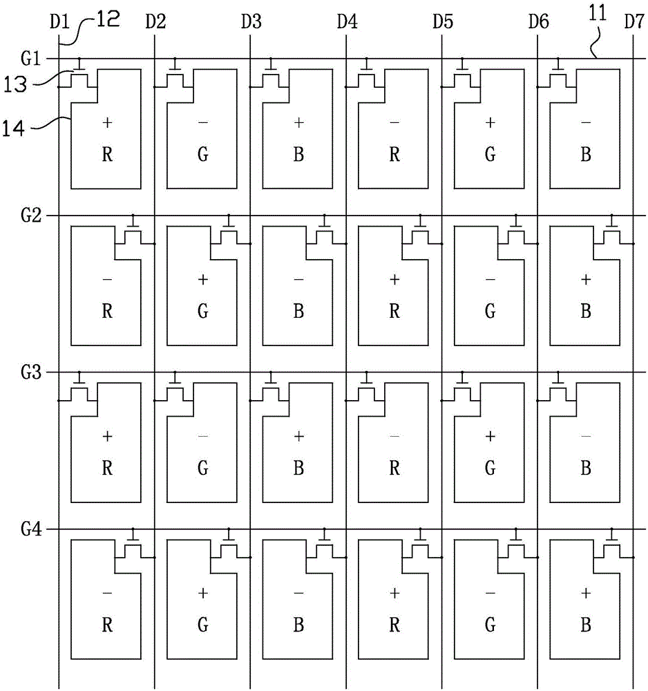
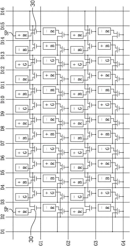
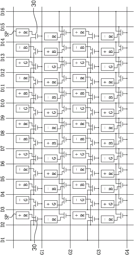
[0046] figure 2 For an equivalent circuit diagram of the pixel array structure in one embodiment of the present invention, please refer to figure 2The pixel array structure includes m scanning lines G1-Gm (only four scanning lines G1-G4 are shown in the figure), n data lines D1-Dn (only sixteen data lines D1-D16 are shown in the figure), and the The m scanning lines and the n data lines intersect each other to define a plurality of sub-pixels (sub-pixels) SP, and the plurality of sub-pixels SP are arranged in a matrix in multiple rows and columns.

[0047] For every two adjacent rows of sub-pixels SP up and down, the sub-pixel SP located between two adjace...


PUM


Abstract

Disclosed is a pixel array structure, a preparing method thereof, and a display panel. The pixel array structure comprises m scanning lines, n USB cables, wherein multiple sub-pixels are formed through reciprocal overlapping restriction by the m scanning lines and the n USB cables, and are arranged into multiple lines and multiple rows in a matrix mode; among the sub-pixels in every adjacent two lines, the sub-pixels which are in one of the two lines and are located between adjacent USB cable Dx and USB cable D (x+1)are connected with USB cable D (x+2), and the sub-pixels which are in the other line and are located between adjacent USB cable Dx and USB cable D(x+1) are connected with USB cable D(x-1); besides, m, n, and x are all positive integers, and 2<=x<=(n-2). By ingeniously arranging connection relations among the sub-pixels and the USB cables, the display panel can realize a displaying effect of dot inversions through a driving mode of column inversions; meanwhile, every USB cable is merely connected with the sub-pixel of the same color, and displaying of a pure color picture only needs the starting of one third of the USB cables, thus the display panel can be more power saving when displaying the pure color picture.

Description

technical field [0001] The invention relates to the field of display technology, in particular to a pixel array structure, a manufacturing method thereof, and a display panel with the pixel array structure. Background technique [0002] Thin film transistor liquid crystal display panel (TFT-LCD) has the advantages of good image quality, small size, light weight, low driving voltage, low power consumption, no radiation and relatively low manufacturing cost, and it occupies a dominant position in the field of flat panel display. [0003] When the liquid crystal display panel is normally displayed, in order to avoid the polarization of the liquid crystal, the voltage applied to the pixel electrode is alternately reversed relative to the common electrode, that is, the voltage of the pixel electrode changes back and forth between positive polarity and negative polarity, which is called inversion drive . When the voltage of the pixel electrode is higher than the voltage of the co...

Claims


Application Information

Patent Timeline
IPC IPC(8): G02F1/1362G02F1/1368H01L27/12H01L21/77
CPCH01L27/124H01L27/1259G02F1/136286G02F1/1368G02F1/136295
Inventor 刘锦李森龙康海燕
Owner KUSN INFOVISION OPTOELECTRONICS
Why Eureka
Try Eureka