Display panel, display and method for manufacturing display panel

A technology for display panels and substrates, applied in instruments, nonlinear optics, optics, etc., can solve problems such as affecting manufacturing costs and manufacturing efficiency, reducing brightness, and inconvenient disassembly and assembly of external control and privacy films. The effect of improving the integration, improving the manufacturing efficiency

Inactive Publication Date: 2017-07-14
TUNGHSU KUNSHAN DISPLAY MATERIAL CO LTD +2
View PDF5 Cites 8 Cited by
  • Summary
  • Abstract
  • Description
  • Claims
  • Application Information

AI Technical Summary

Problems solved by technology

[0003] With the development of display technology, people have new requirements for the versatility of the display, not only requiring brightness, clear picture quality, etc., but also requiring privacy protection. The current method is to install an external anti-peeping film to protect the user's privacy. Information, but the thickness of the anti-spy film is about 2mm, and the brightness decreases by about 30% after use, which in turn affects the display quality, and the structure of this anti-external control anti-spy film is very inconvenient to disassemble, which affects manufacturing Cost and Manufacturing Efficiency

Method used


Image

  • Display panel, display and method for manufacturing display panel
  • Display panel, display and method for manufacturing display panel
  • Display panel, display and method for manufacturing display panel

Examples


Embodiment Construction

[0028] Specific embodiments of the present invention will be described in detail below in conjunction with the accompanying drawings. It should be understood that the specific embodiments described here are only used to illustrate and explain the present invention, and are not intended to limit the present invention.

[0029] In the following description of the present invention, the "front" and "back" of the CF substrate are terms introduced to illustrate the structure of the display panel, and the "front" is relative to the "back", but this is not used to limit Within the scope of the present invention, those skilled in the art may replace it with other terms that can clearly describe the structure of the display panel.

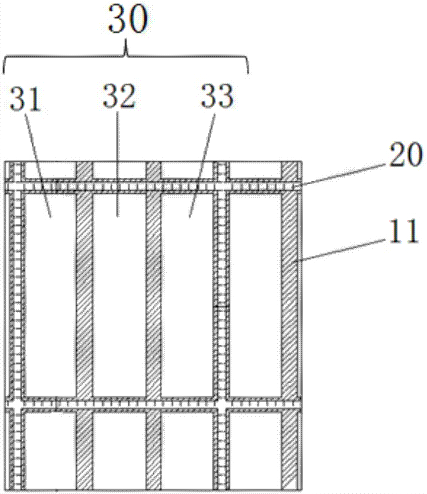
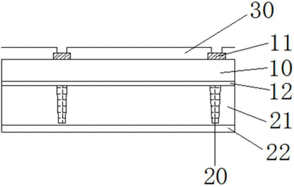
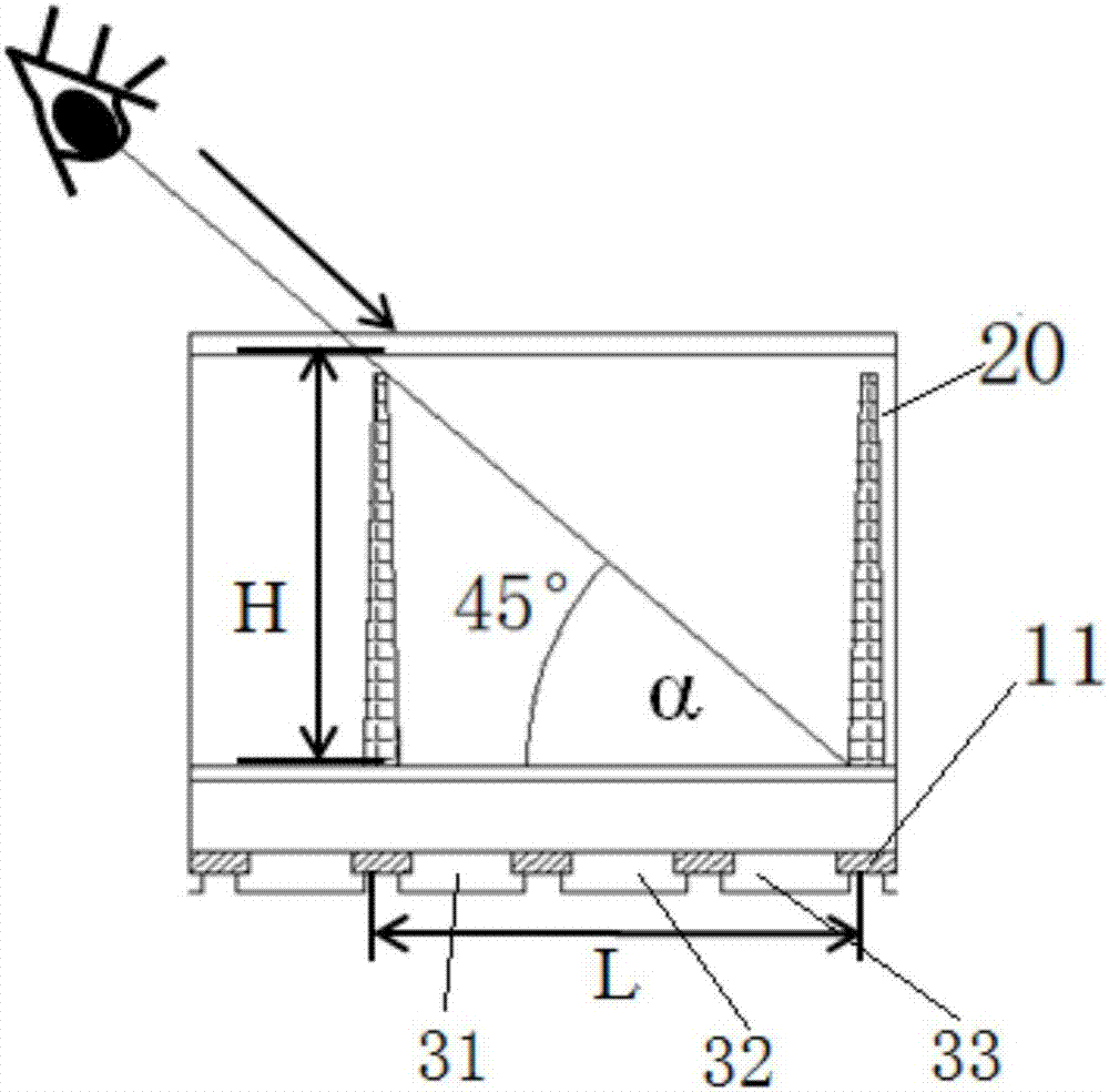
[0030] figure 1 is a schematic diagram of the basic structure of a CF substrate of a display panel according to an embodiment of the present invention. like figure 1 As shown, a plurality of pixels 30 and a black matrix 11 are formed on the front of the ...


PUM

PropertyMeasurementUnit
thicknessaaaaaaaaaa

Abstract

The invention relates to the technical field of displaying, and discloses a display panel. The display panel comprises a CF (Colour Filter) substrate, wherein a plurality of pixel points are formed on the front side of the CF substrate; one pixel point comprises a plurality of sub-pixels. The display panel is characterized by comprising a first transparent conductive layer, a second transparent conductive layer, an electrochromic structure and a solid electrolyte, wherein the electrochromic structure is formed by an electrochromic material, and has a certain height; the first transparent conductive layer is formed on the back side of the CF substrate; the electrochromic structure and the solid electrolyte are formed between the first transparent conductive layer and the second transparent conductive layer; the solid electrolyte is formed on the periphery of the electrochromic structure. The invention further provides a display including the display panel and a method for manufacturing the display panel. Through the scheme of the invention, a visual angle can be controlled while the display quality is not influenced, and integration and thinning are facilitated.

Description

technical field [0001] The invention relates to the field of displays, in particular to a display panel, a display and a method for manufacturing the display panel. Background technique [0002] With the evolution of semiconductor technology, the development of flat-panel displays has also been driven. Among many types of flat-panel displays, liquid crystal displays have gradually become the mainstream of the market due to their low space occupation, low power consumption, low radiation, and low electromagnetic interference. The liquid crystal display includes a TFT (Thin Film Transistor) substrate as the upper substrate and a CF (Colour Filter, color filter) substrate as the lower substrate. Liquid crystals are injected between the TFT substrate and the CF substrate, and the TFT substrate is formed to control the deflection of the liquid crystal. In the thin film transistor circuit, red, green, blue light filter structures and other structures are formed on the CF substrate...

Claims


Application Information

Patent Timeline
Patent Type & Authority Applications(China)
IPC IPC(8): G02F1/1333G02F1/1343G02F1/153
CPCG02F1/1333G02F1/134309G02F1/153
Inventor 许非凡刘海亮王鹏涛严清涛
Owner TUNGHSU KUNSHAN DISPLAY MATERIAL CO LTD
Why Eureka
Try Eureka