Display panel and manufacturing method thereof

A technology of a display panel and a manufacturing method, which is applied in nonlinear optics, instruments, optics, etc., can solve the problems of pixel point burrs and the inability of liquid crystal molecules to align stably, and achieve the effects of reducing dark alignment patterns and line widths

Active Publication Date: 2018-02-13
SHENZHEN CHINA STAR OPTOELECTRONICS TECH CO LTD
View PDF5 Cites 4 Cited by
  • Summary
  • Abstract
  • Description
  • Claims
  • Application Information

AI Technical Summary

Problems solved by technology

In the PSVA production process, there is an overlapping part between the color resist edge of the pixel and the black matrix, and the overlapping part is in each pixel ...

Method used


Image

  • Display panel and manufacturing method thereof
  • Display panel and manufacturing method thereof
  • Display panel and manufacturing method thereof

Examples


Embodiment Construction

[0025] The present invention will be described in further detail below in conjunction with the accompanying drawings and embodiments.

[0026] Figure 1-5 What is shown in is only the film layer or electrode structure related to the present invention, wherein the thickness and size of layers and regions are omitted or exaggerated, but it is worth noting that the schematic drawings and embodiments shown in conjunction with the accompanying drawings It is intended to explain the principles of the invention and its practical application, thereby enabling others skilled in the art to understand various embodiments of the invention and various modifications as are suited to particular intended uses.

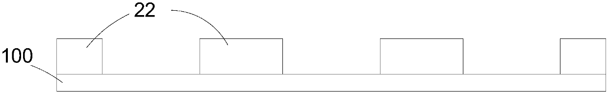
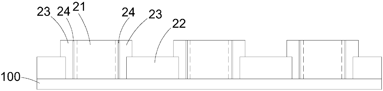
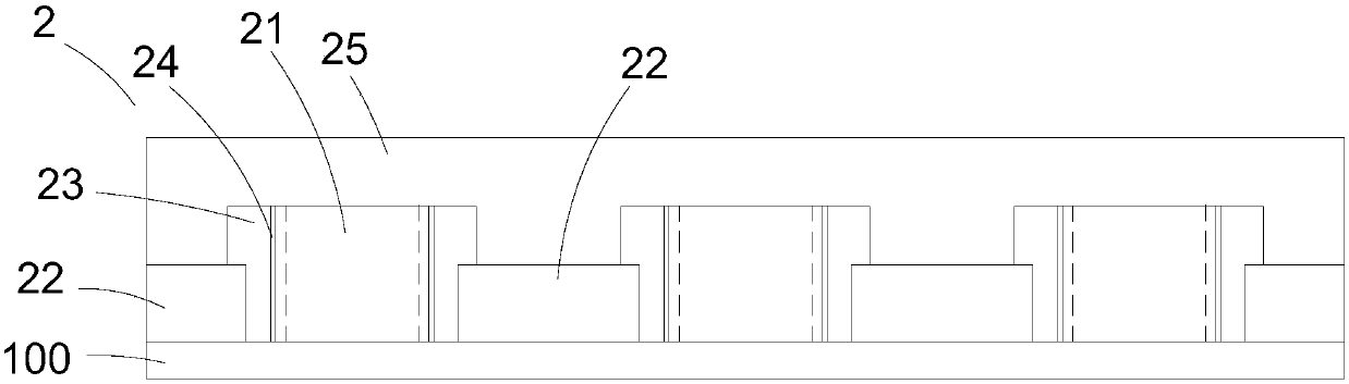
[0027] Such as Figure 5 As shown, a display panel of the present invention, where the display mode of the display panel is PSVA display mode, the display panel includes an array substrate 1 and a color filter substrate 2, the array substrate 1 and the color filter substrate 2 is pr...


PUM

PropertyMeasurementUnit
Widthaaaaaaaaaa

Abstract

The invention provides a display panel. The display panel includes an array substrate and a colorful filter substrate; the colorful filter substrate comprises color resistors and a black matrix; an extension area is arranged between the periphery of each color resistor and the black matrix, and is internally provided with first insulating electrodes made of conductive materials; the array substrate comprises pixel electrodes corresponding to the color resistors in a one-to-one mode, the outer circumference of each pixel electrode is provided with a circle of second insulating electrodes opposite to the first insulating electrodes in position, and the second insulating electrodes are not in contact with the pixel electrodes; the voltage applied on the first insulating electrodes is equal tothat applied on the second insulating electrodes. The invention further provides a manufacturing method of the display panel. Compared with the prior art, the occurrence of aligning dark fringes at the edges of the pixel electrodes is reduced.

Description

technical field [0001] The invention relates to a liquid crystal panel technology, in particular to a display panel and a manufacturing method thereof. Background technique [0002] At present, a liquid crystal display panel usually includes a color filter substrate (CF substrate), an array substrate (TFT substrate), and a liquid crystal (LC) filled between the color filter substrate and the array substrate to form a liquid crystal cell, in which PSVA (PolmerStabilized Vertically Aligned (polymer stabilized vertically aligned liquid crystal) display mode, as a PSA technology, has the advantages of high contrast, wide viewing angle, fast response and low power consumption. It is one of the display modes used by mainstream liquid crystal display panels at present; The principle is that, firstly, a power source is used to deflect the liquid crystal molecules, and then anchored by ultraviolet light (UV) to complete the alignment of the liquid crystals. In the PSVA production pr...

Claims


Application Information

Patent Timeline
IPC IPC(8): G02F1/1343G02F1/1335G02F1/1333
CPCG02F1/1333G02F1/133512G02F1/133514G02F1/1343G02F1/13439
Inventor 项小群
Owner SHENZHEN CHINA STAR OPTOELECTRONICS TECH CO LTD
Why Eureka
Try Eureka