Array substrate and display device

An array substrate and substrate technology, applied in optics, instruments, electrical and digital data processing, etc., can solve problems such as affecting display effect, uneven pressing, and poor touch.

Active Publication Date: 2018-07-06
XIAMEN TIANMA MICRO ELECTRONICS
View PDF5 Cites 10 Cited by
  • Summary
  • Abstract
  • Description
  • Claims
  • Application Information

AI Technical Summary

Problems solved by technology

[0004] The present invention provides an array substrate and a display device to solve the problems of uneven pressing affecting the display effect and poor touch

Method used


Image

  • Array substrate and display device
  • Array substrate and display device
  • Array substrate and display device

Examples


Embodiment Construction

[0024] The present invention will be further described in detail below in conjunction with the accompanying drawings and embodiments. It should be understood that the specific embodiments described here are only used to explain the present invention, but not to limit the present invention. In addition, it should be noted that, for the convenience of description, only some structures related to the present invention are shown in the drawings but not all structures. Throughout this specification, the same or similar reference numerals represent the same or similar structures, elements or processes. It should be noted that, in the case of no conflict, the embodiments in the present application and the features in the embodiments can be combined with each other.

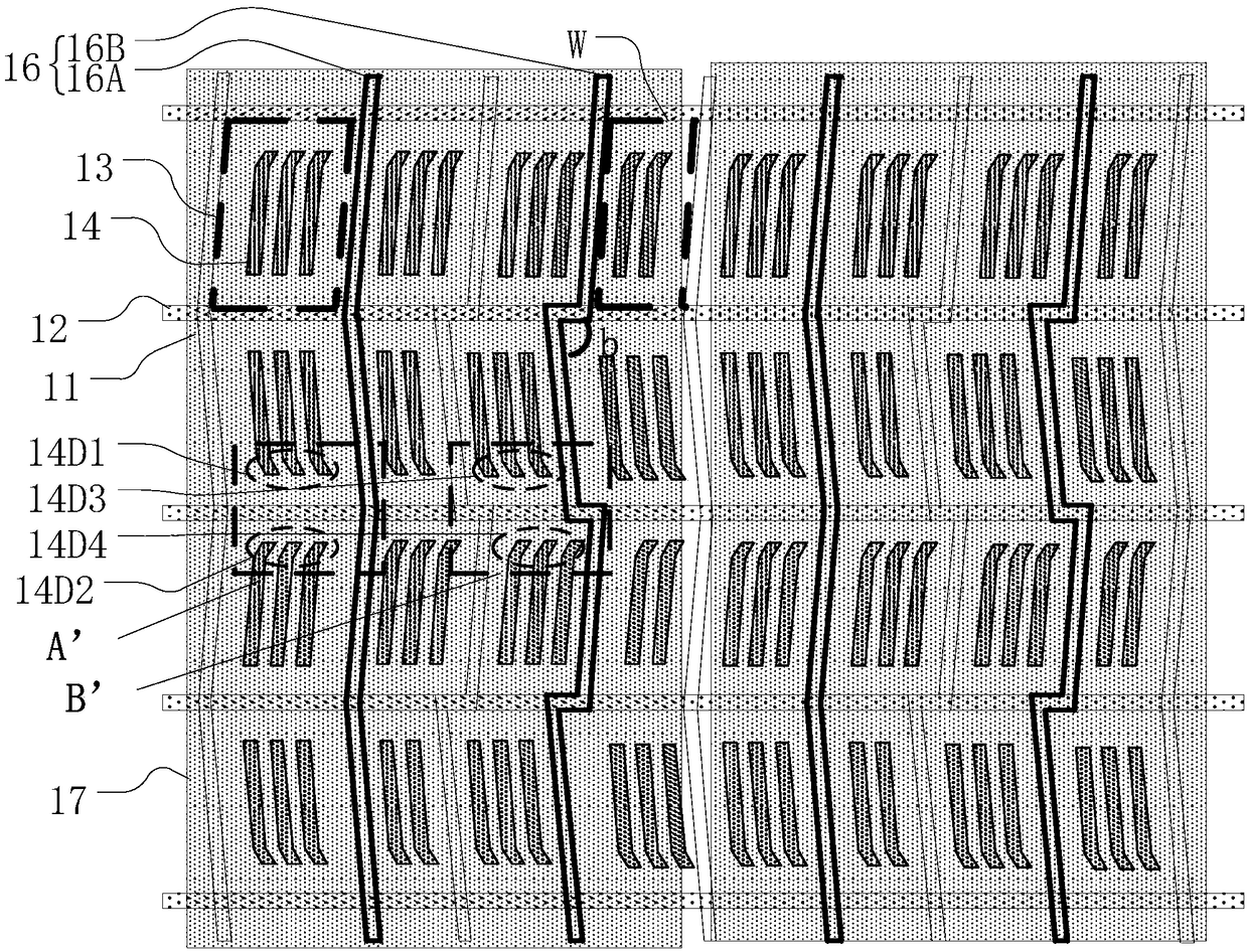
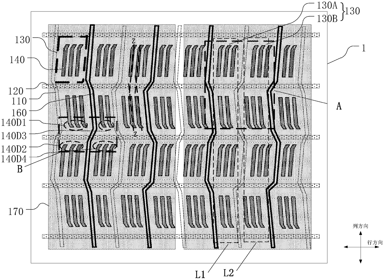
[0025] At present, pseudo-dual domain technology is widely used in IPS technology and FFS technology, figure 1 It is a schematic plan view of an array substrate applying pseudo-dual domain technology. Data lines 11 and...


PUM


Abstract

An embodiment of the invention discloses an array substrate and a display device. The array substrate comprises a substrate body, and multiple scanning lines and multiple data lines are arranged on the substrate body to form multiple subpixels in intersection; pixel electrodes arranged in the subpixels include multiple stripline electrodes, long axes of the stripline electrodes in the same row ofthe subpixels are parallelly mutually, and the long axes of the stripline axles in any two rows of the subpixels extend in intersection; each touch electrode is electrically connected with at least one touch signal line, each touch signal line comprises multiple straight line parts and multiple folding line parts, the two neighboring straight line parts are connected through the folding line parts, the straight line parts are parallel to the long axles of the stripline electrodes located in the same raw of the subpixels, extending lines of the folding line parts interact the long axes of the stripline electrodes, and orthographic projection of the folding line parts on the substrate body overlap with that of the scanning lines on the substrate while the folding line parts are not perpendicular to the scanning lines. By the arrangement, the problem that display effect is affected by uneven pressure.

Description

technical field [0001] Embodiments of the present invention relate to the field of display technology, and in particular, to an array substrate and a display device. Background technique [0002] In the field of liquid crystal display technology, in-plane switching (In-Plane Switching IPS) technology and fringe field switching (Fringe Field Switching FFS) technology are two commonly used wide viewing angle liquid crystal display technologies, which are characterized by pixel electrodes and common electrodes. It is arranged on the same substrate to make the liquid crystal molecules rotate in a plane parallel to the substrate, thereby improving the light transmission efficiency of the liquid crystal layer. Especially in the field of liquid crystal display technology with built-in touch, based on IPS or FFS technology, using mutual capacitance or self-capacitance mode to divide common electrodes into touch blocks for time-sharing touch technology has become the mainstream. [...

Claims


Application Information

Patent Timeline
Patent Type & Authority Applications(China)
IPC IPC(8): G02F1/1362G02F1/1333
CPCG02F1/13338G02F1/1362G02F1/136222G02F1/134363G06F3/0412G06F3/0448G02F1/134309G02F1/134336G02F1/13439G02F1/136286G02F2201/121G02F2201/122G02F2201/123G02F2201/52G06F3/044G02F1/134345
Inventor 郭珂伍黄尧周洪波曹兆铿路璇杨康鹏许育民
Owner XIAMEN TIANMA MICRO ELECTRONICS
Why Eureka
Try Eureka