A kind of array substrate and display panel

A technology for array substrates and display panels, which is applied to semiconductor/solid-state device parts, instruments, semiconductor devices, etc., can solve problems such as abnormal resistance, open circuit or short circuit, and affect the yield rate of thin film transistor liquid crystal display products, so as to reduce static electricity. The probability of injury and the effect of improving product yield

Active Publication Date: 2020-04-10
SHENZHEN CHINA STAR OPTOELECTRONICS SEMICON DISPLAY TECH CO LTD
View PDF5 Cites 0 Cited by
  • Summary
  • Abstract
  • Description
  • Claims
  • Application Information

AI Technical Summary

Problems solved by technology

[0003] However, in the manufacturing process of thin film transistor liquid crystal display, it needs to go through a lot of equipment and process. During the manufacturing process, a large amount of static electricity will be accumulated on the glass substrate, resulting in electrostatic damage to large and long metal design traces, making the Its abnormal resistance value, open circuit or short circuit directly affects the yield rate of thin film transistor liquid crystal display products

Method used


Image

  • A kind of array substrate and display panel
  • A kind of array substrate and display panel
  • A kind of array substrate and display panel

Examples


Embodiment 1

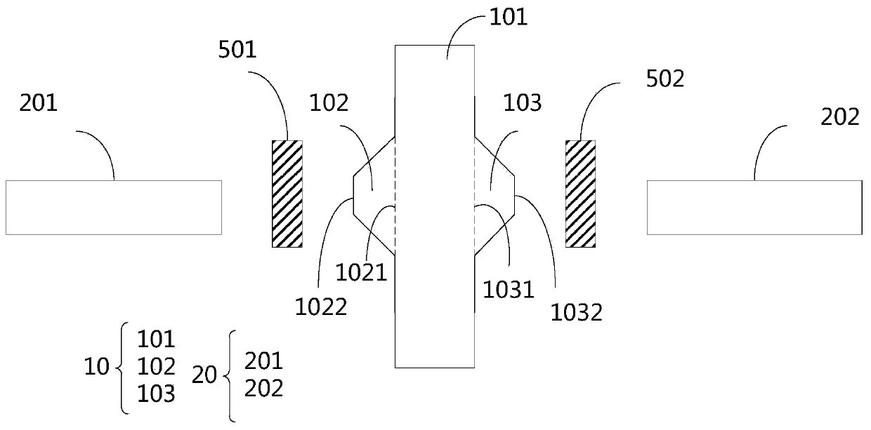
[0023] see figure 1 , figure 1 Schematic diagram of the wiring plane structure of the array substrate provided for the embodiment of the present invention Figure 1 . An embodiment of the present invention provides an array substrate, including:

[0024] The first trace 10 and the second trace 20; wherein, the first trace 10 includes a main body 101 and a first protruding portion 102, and the first protruding portion 102 is arranged on the main body 101 close to the second trace On one side of the wire 20; the second wire 20 is arranged opposite to the first protruding portion 102, and a first electrostatic protection electrode 501 is arranged between the second wire 20 and the protruding portion 102, So that electrostatic damage occurs on the first electrostatic protection electrode 501 .

[0025] The first routing 10 separates the second routing 20 into a first part 201 and a second part 202, the first routing further includes a second protrusion 103, and the first protr...

Embodiment 2

[0035] The array substrate according to the first embodiment will be further described in detail below with an example.

[0036] The array substrate provided by the embodiments of the present invention may be implemented in combination with one or more first wirings and one or more second wirings.

[0037] In this embodiment, it will be described by taking that there is one first wiring and two second wirings on the array substrate as an example.

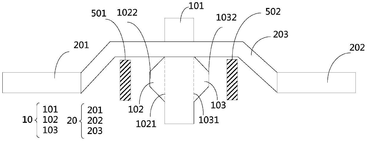
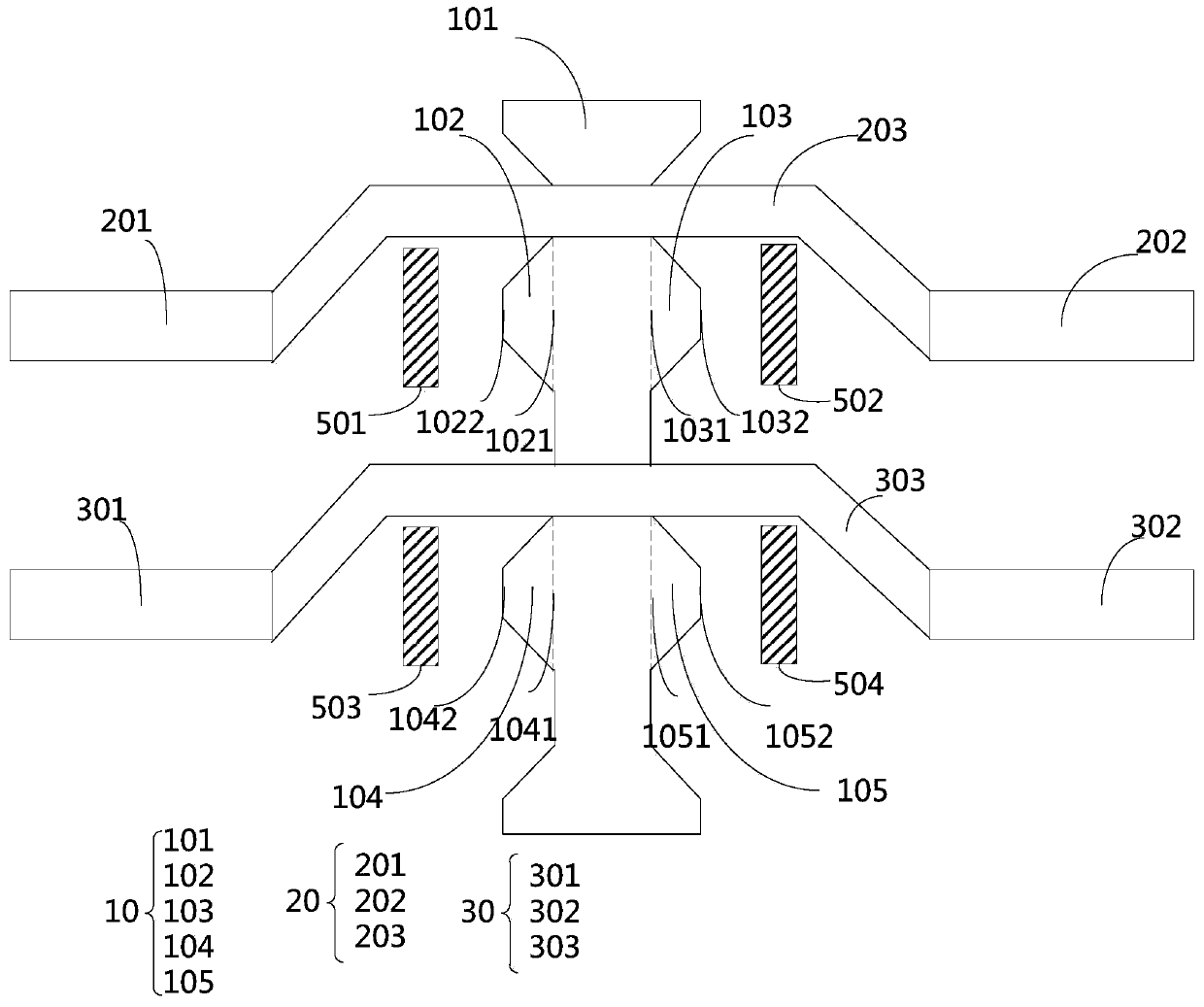
[0038] see image 3 , image 3 A schematic plan view of a partial wiring area of ​​an array substrate provided by a preferred embodiment of the present invention.

[0039] An embodiment of the present invention provides an array substrate, including:

[0040]The first wiring 10, the second wiring 20 and the third wiring 30;

[0041] Specifically, the first wiring 10 may be a peripheral wiring or a common electrode line, the second wiring 20 may be a scanning line or a common electrode line, and the third wiring 30 may be a scann...


PUM


Abstract

The invention provides an array substrate and a display panel. The array substrate comprises a first routing and a second routing, wherein the first routing comprises a main body part and a first projection part, and the first projection part is arranged on the side, close to the second wiring, of the main body part; the second wiring and the first projection part are oppositely arranged, and a first electrostatic protection electrode is arranged between the second wiring and the first projection part. The array substrate has the beneficial effects that, according to the array substrate and the display panel provided by the invention, the probability of damage by static electricity can be reduced, namely metal routings required in the panel cannot be influenced even if the damage by staticelectricity occurs, so that the product yield is improved.

Description

technical field [0001] The present invention relates to the field of display technology, in particular to an array substrate and a display panel. Background technique [0002] In the TFT-LCD panel design, a large number of signals need to use metal wiring to connect to the peripheral drive circuit, so that the external drive signal and pulse timing signal are provided to the panel pixel area for display and drive. In the peripheral circuit traces, the most commonly used bulk and strip metal designs are used to reduce parasitic resistance and parasitic capacitance. [0003] However, in the manufacturing process of thin-film transistor liquid crystal displays, a lot of equipment and processes are required, and a large amount of static electricity will be accumulated on the glass substrate during the manufacturing process, resulting in electrostatic damage to large and long metal design traces, making the Abnormal resistance, open circuit or short circuit directly affect the y...

Claims


Application Information

Patent Timeline
Patent Type & Authority Patents(China)
IPC IPC(8): H01L23/60H01L27/12G02F1/1362
CPCG02F1/136204G02F2202/22H01L23/60H01L27/124
Inventor 李珊陈书志
Owner SHENZHEN CHINA STAR OPTOELECTRONICS SEMICON DISPLAY TECH CO LTD
Why Eureka
Try Eureka