Large-Scale Integrated Optical Switch Chip Based on Optical Phased Array

A technology for large-scale integration of optical and optical phased arrays, applied in the field of optical phased arrays, to achieve the effects of increased scalability, low power consumption, and low crosstalk

Active Publication Date: 2020-10-16
SHANGHAI JIAO TONG UNIV +1
View PDF10 Cites 0 Cited by
  • Summary
  • Abstract
  • Description
  • Claims
  • Application Information

AI Technical Summary

Problems solved by technology

[0004] The present invention is based on the existing photonics theory and phased array technology. Aiming at the problems faced by the traditional planar integrated waveguide optical switch, a large-scale integrated optical switch chip based on phased array is proposed. The integrated optical switch chip has strict Non-blocking, high-speed, low insertion loss, low crosstalk, etc., can meet the needs of optical communication and optical interconnection network for large-capacity data exchange

Method used


Image

  • Large-Scale Integrated Optical Switch Chip Based on Optical Phased Array
  • Large-Scale Integrated Optical Switch Chip Based on Optical Phased Array
  • Large-Scale Integrated Optical Switch Chip Based on Optical Phased Array

Examples


Embodiment Construction

[0020] The embodiments of the present invention are described in detail below in conjunction with the accompanying drawings. This embodiment is implemented on the premise of the technical solution of the present invention, and detailed implementation methods and operating procedures are provided, but the protection scope of the present invention is not limited to the following Example.

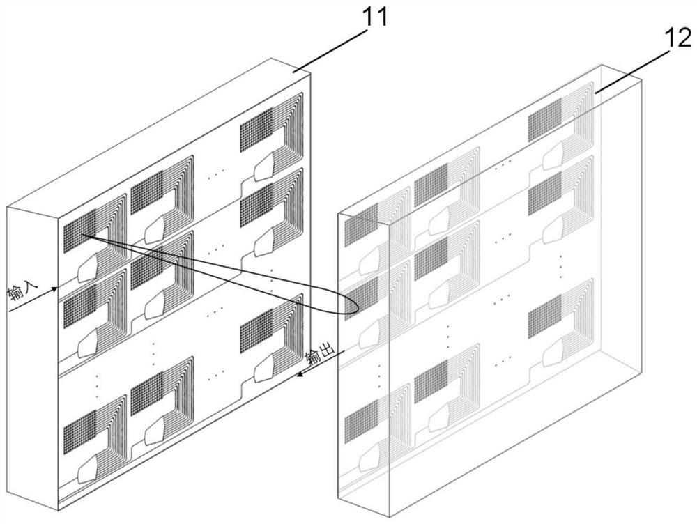
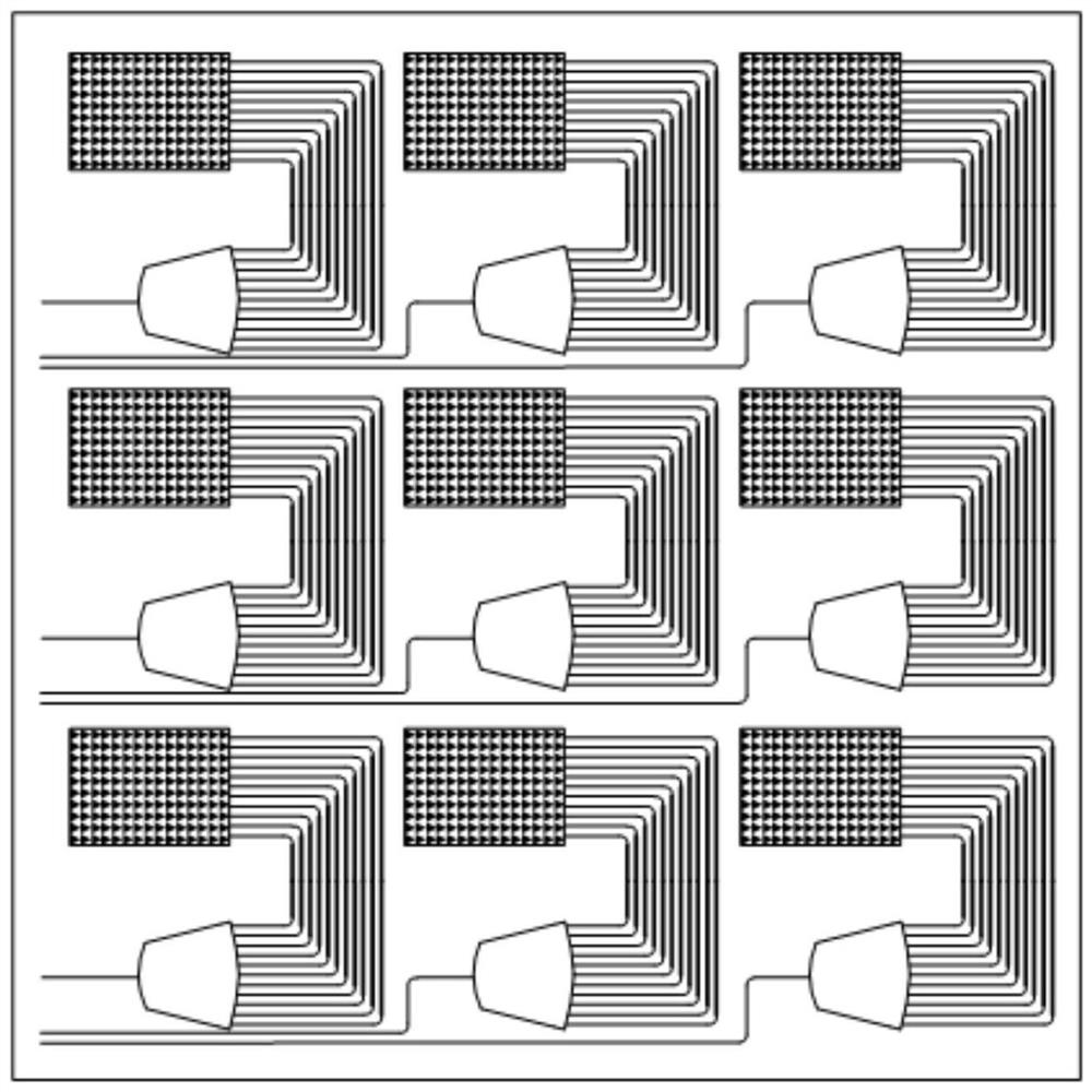
[0021] figure 1 It is a structural schematic diagram of the optical phased array-based large-scale integrated optical switch chip of the present invention. It can be seen from the figure that the optical switch includes a silicon-based phased-array receiving chip 11 and a silicon-based phased-array transmitting chip 12, which are relatively parallel placed. The silicon-based phased-array receiving chip 11 consists of N×N The optical phased array unit forms a two-dimensional array, and each optical phased array unit is composed of a beam splitter 1 at the front entrance, an intermediate phase ...


PUM


Abstract

A large-scale integrated optical switch chip based on an optical phased array is characterized by comprising a silicon-based phased array emission chip and a silicon-based phased array reception chipwhich are arranged opposite to each other and in parallel, the silicon-based phased array emission chip includes a 2D array composed of N*N optical phased array units, and each optical phased array unit is composed of a light beam splitter in a front input port, a phase modulator in the middle and a light emitting port in the tail end. The large-scale integrated optical switch chip is characterized by being completely free of obstruction, high in speed, low in insertion loss and low in crosstalk, and can satisfy requirement for large capacity data exchange of optical communication and opticalinterconnection network.

Description

technical field [0001] The invention relates to an optical phased array, in particular to a large-scale integrated optical switch chip based on the phased array. Background technique [0002] The continuous development of the Internet puts forward higher requirements on the data transmission bandwidth and delay of the optical fiber network. Traditional mechanical optical switches are slow, bulky, difficult to integrate on a large scale, and difficult to adapt to the transmission requirements of optical transport networks. In addition to being used in optical fiber transmission backbone networks, integrated optical switches will also play an important role in optical interconnection networks for computers and data centers. Optical phased array is developed on the basis of traditional microwave phased array, and it is a new type of beam shaping and pointing control method. The optical phased array can work in the near-infrared band or even the visible light band. Compared w...

Claims


Application Information

Patent Timeline
Patent Type & Authority Patents(China)
IPC IPC(8): G02B6/12
CPCG02B6/12009G02B2006/12145
Inventor 周林杰沈林陆梁军陈建平刘娇
Owner SHANGHAI JIAO TONG UNIV
Why Eureka
Try Eureka