Design method of layout at board card golden finger and server board card

A server board and design method technology, applied in computer design circuit, CAD circuit design, instrument and other directions, can solve the problems of low quality of high-speed signal transmission and high bit error rate of signal transmission

Active Publication Date: 2018-12-07
SUZHOU LANGCHAO INTELLIGENT TECH CO LTD
View PDF3 Cites 2 Cited by
  • Summary
  • Abstract
  • Description
  • Claims
  • Application Information

AI Technical Summary

Problems solved by technology

[0006] This application provides a layout design method at the gold finger of the board and a server board to solve the problems of low transmission quality of some high-speed signals and high bit error rate of signal transmission due to the layout design method in the prior art

Method used


Image

  • Design method of layout at board card golden finger and server board card
  • Design method of layout at board card golden finger and server board card
  • Design method of layout at board card golden finger and server board card

Examples


Embodiment 1

[0042] see Figure 5 , Figure 5 It is a schematic flow chart of a method for designing a layout at a golden finger of a board provided by an embodiment of the present application. Depend on Figure 5 It can be seen that the layout design method of the golden finger of the board in this application mainly includes the following process:

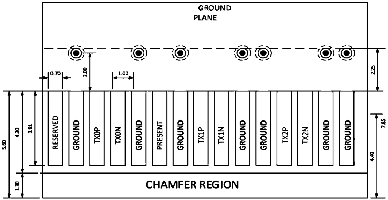
[0043] S1: According to the type of the GND pin on the gold finger of the board and the space between the gold finger and the GND via on the board, set the number of GND vias interconnected with the GND pin so that the GND pins can be interconnected GND via reaches the maximum number.

[0044] see Figure 6 , Figure 6 for Figure 6 It is a schematic structural diagram of the layout wiring at the golden finger in the embodiment of the present application. Generally, there are two types of GND pins on the gold fingers of server boards: single GND pins and double GND pins. Depend on Figure 6 It can be seen that, in this embodiment, th...

Embodiment 2

[0055] The present application also provides a server board, the server board includes a gold finger, and the layout design of the gold finger is carried out by the above-mentioned method. Specifically, multiple groups of GND pins are provided on the golden finger, and each group of GND pins is combined and interconnected with two or more GND vias to form a signal return path.

[0056] Among them, the GND pins on the golden finger include single-pin GND pins and double-pin GND pins. In the server board, the number of GND vias set for different types of GND pins is different. Any single GND pin and two GND vias are combined and interconnected to form a signal return path; any double GND pin is connected to three The GND vias are combined and interconnected to form a signal return path.

[0057] In any signal return path in this application, all GND vias are closely adjacent to the GND pins in the signal return path.

[0058] Further, in a signal return path, the distance betw...


PUM


Abstract

The present invention discloses a design method of layout at a board card golden finger and a server board card. The design method comprises the steps of: setting the quantity of GND via interconnected with GND pins according to the types of the GND pins on the board card golden finger and a space between a golden finger on the board card and the GND vias to allow the GND vias interconnected withthe GND pins to reach the maximum quantity; and combining and interconnecting the GND pins with all the GND vias matched with the GND pins to form a signal return path; in the signal return path, getting all the GND vias tightly close to the matching GND pins to minimize the length of the signal return path. The design method can greatly reduce the degree of attenuation in the transmission processof high-speed signals and can effectively optimize the signal return path so as to avoid generation of resonance points on a high-frequency section by a signal insertion loss waveform, near-end cross-talk frequency domain waveform and far-end cross-talk frequency domain waveform, facilitate improvement of the quality of signal transmission and improve the operation stability of the whole system.

Description

technical field [0001] The present application relates to the technical field of server board design, in particular to a design method of a gold finger layout of a board and a server board. Background technique [0002] In the field of server board design, with the increase of the high-speed interface rate, the transmission quality of high-speed signals in the channel link has attracted people's attention, and the layout design of the golden finger of the server board closely affects the transmission of high-speed signals Therefore, it is an important issue to study the wiring design of the layout at the golden finger of the server board. [0003] For the current wiring design method of the golden finger of the server board, please refer to figure 1 . Depend on figure 1 It can be seen that the current layout design method for the gold finger of the server board is mainly: each GND pin of the gold finger corresponds to a GND pin, and the GND pin of the gold finger and the ...

Claims


Application Information

Patent Timeline
Patent Type & Authority Applications(China)
IPC IPC(8): H05K3/00H05K1/02G06F17/50
CPCH05K1/0218H05K1/0237H05K3/0002H05K3/0005G06F30/39G06F30/392H01R12/721
Inventor 武宁
Owner SUZHOU LANGCHAO INTELLIGENT TECH CO LTD
Why Eureka
Try Eureka