Array substrate and liquid crystal display panel

An array substrate, thin film transistor technology, applied in nonlinear optics, instruments, optics, etc., to achieve the effects of low color shift, reduced aperture ratio, and simple structure

Active Publication Date: 2018-12-14
SHENZHEN CHINA STAR OPTOELECTRONICS SEMICON DISPLAY TECH CO LTD
View PDF5 Cites 1 Cited by
  • Summary
  • Abstract
  • Description
  • Claims
  • Application Information

AI Technical Summary

Problems solved by technology

However, in the liquid crystal display panel with this structure, the data signal input is doubled, and the number of source driver (source) ICs is doubled.

Method used


Image

  • Array substrate and liquid crystal display panel
  • Array substrate and liquid crystal display panel
  • Array substrate and liquid crystal display panel

Examples


Embodiment Construction

[0014] The array substrate and liquid crystal display panel provided by the present invention will be described in detail below with reference to the accompanying drawings. Apparently, the described embodiments are only some of the embodiments of the present invention, but not all of them. Based on the embodiments of the present invention, all other embodiments obtained by persons of ordinary skill in the art without making creative efforts belong to the protection scope of the present invention.

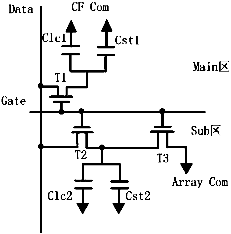
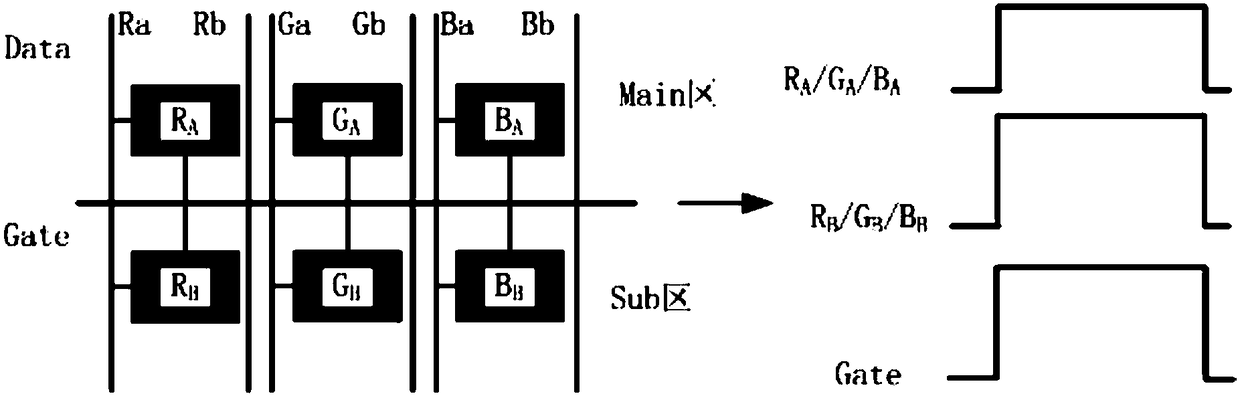
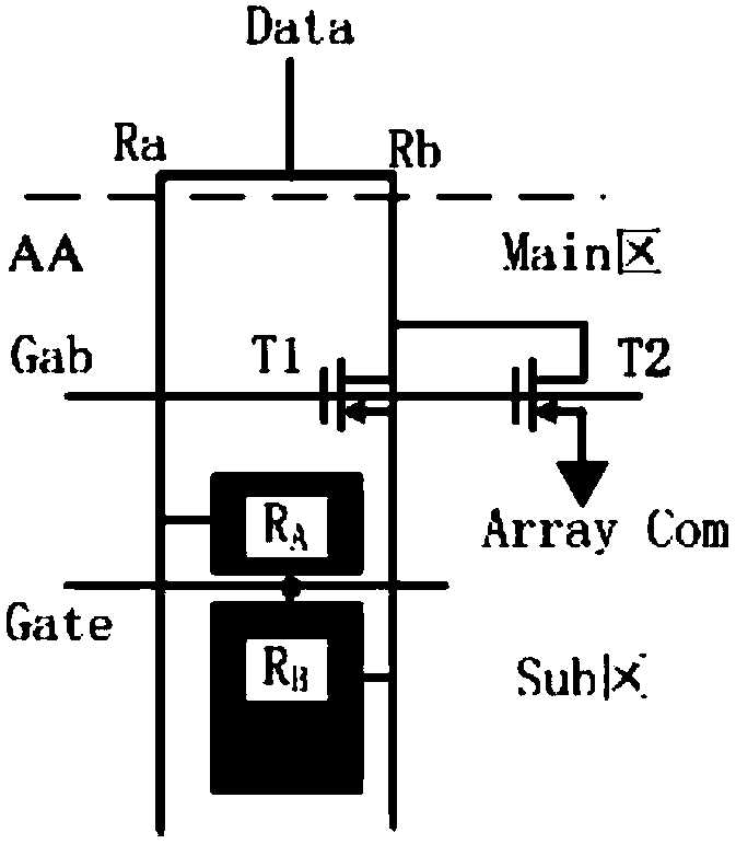
[0015] The array substrate of the present invention includes: a scanning line (Gate) and a data line (Data); each of the data lines is split into a first data line and a second data line before entering the display area (AA); The scanning line and the adjacent first data line and the second data line define a pixel area, and the pixel electrode of each pixel area includes a main area electrode and a sub area electrode, and the first data line provides the main area electrode The fi...


PUM


Abstract

The invention provides an array substrate and a liquid crystal display panel. A first and second data lines defining pixel areas share one data signal and are divided into two lines before entering adisplay area. A pixel electrode of each pixel area comprises a primary area electrode and a secondary area electrode, two thin film transistors are formed in the area where the primary area electrodeis located, and opening of the two thin film transistors is controlled by a grid control signal, so that voltage applied to the secondary area electrode is changed, the voltage applied to the primaryarea electrode and the voltage applied to the secondary area electrode form a preset ratio, and liquid crystal molecules in the two areas have different dumping degrees, so that a low color shift effect is achieved. Three thin film transistors are not required in each pixel area, the structure is simpler, the aperture ratio is not reduced, and the number of source IC is not required to be increased.

Description

technical field [0001] The invention relates to the technical field of liquid crystal display, in particular to an array substrate and a liquid crystal display panel capable of realizing low color shift (Low ColorShift). Background technique [0002] With the development of optoelectronic and semiconductor technologies, liquid crystal displays (Liquid Crystal Display, LCD) are also developing vigorously. Among many liquid crystal displays, a thin film transistor liquid crystal display (Thin Film Transistor Liquid Crystal Display, TFT-LCD) has superior characteristics such as high space utilization efficiency, low power consumption, no radiation, and low electromagnetic interference. In the field of display technology, LCS (Low Color Shift) technology mainly reduces the color cast caused by viewing images at different angles by improving the structure of the liquid crystal panel. [0003] refer to figure 1 , a schematic diagram of an equivalent circuit of a pixel region of ...

Claims


Application Information

Patent Timeline
Patent Type & Authority Applications(China)
IPC IPC(8): G02F1/1362G02F1/1343
CPCG02F1/134309G02F1/136286G02F1/136222
Inventor 刘林峰
Owner SHENZHEN CHINA STAR OPTOELECTRONICS SEMICON DISPLAY TECH CO LTD
Why Eureka
Try Eureka