Display panel and manufacturing method thereof

A display panel and plane technology, applied in semiconductor devices, electrical components, circuits, etc., can solve the problems of inconsistent color shift in four directions of organic light-emitting display panels

Inactive Publication Date: 2020-07-17
WUHAN TIANMA MICRO ELECTRONICS CO LTD
View PDF7 Cites 5 Cited by
  • Summary
  • Abstract
  • Description
  • Claims
  • Application Information

AI Technical Summary

Problems solved by technology

[0004] Embodiments of the present invention provide a display panel and a manufacturing method thereof, so as to ...

Method used


Image

  • Display panel and manufacturing method thereof
  • Display panel and manufacturing method thereof
  • Display panel and manufacturing method thereof

Examples


Embodiment Construction

[0028] The present invention will be further described in detail below in conjunction with the accompanying drawings and embodiments. It should be understood that the specific embodiments described here are only used to explain the present invention, but not to limit the present invention. In addition, it should be noted that, for the convenience of description, only some structures related to the present invention are shown in the drawings but not all structures.

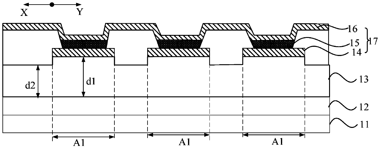
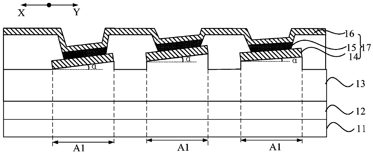
[0029] An embodiment of the present invention provides a display panel, including: a substrate;

[0030] a driving circuit layer disposed on one side of the substrate;

[0031] a planarization layer disposed on a side of the driving circuit layer away from the substrate;

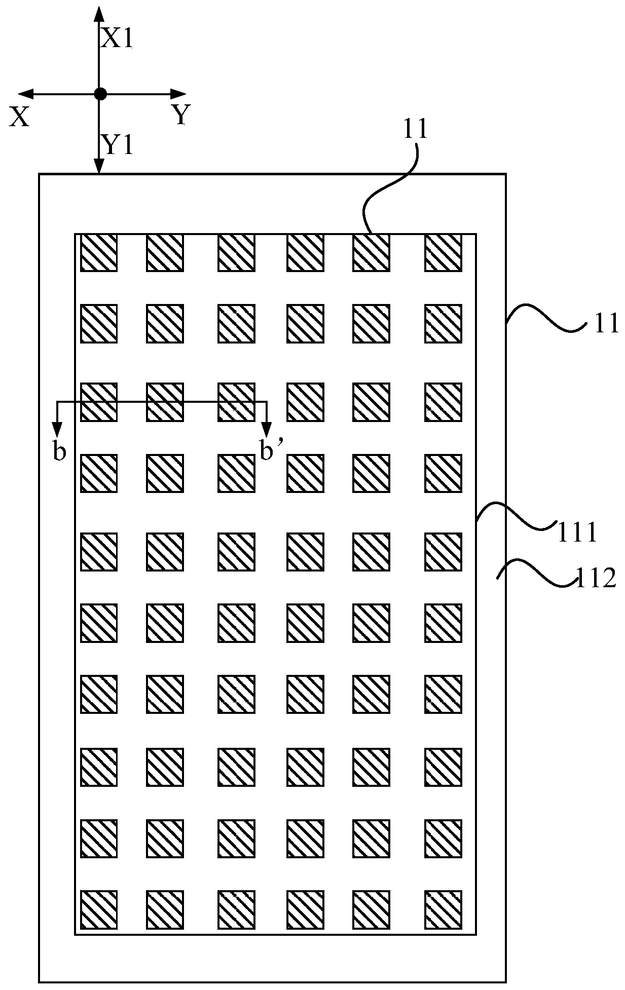
[0032] The first electrode, the light-emitting functional layer and the second electrode are sequentially arranged on the side of the planarization layer away from the substrate; in a plane parallel to the substrate, a plurality of first electr...


PUM

PropertyMeasurementUnit
Thicknessaaaaaaaaaa
Thicknessaaaaaaaaaa

Abstract

The invention discloses a display panel and a manufacturing method thereof. The display panel comprises a substrate; a driving circuit layer which is arranged on the substrate; a planarization layer arranged on the driving circuit layer; first electrodes, light-emitting function layers and second electrodes which are sequentially arranged on the planarization layer, wherein in a plane parallel tothe substrate, the plurality of first electrodes are arranged in an array, the area covered by the orthographic projection of the first electrodes on the substrate is a first area, and the first electrodes are in one-to-one correspondence with the first areas. The surface, close to the first electrode, of the planarization layer of each first area is parallel to the plane where the substrate is located, or, a first inclination angle is formed between the surface, close to the first electrode, of the planarization layer of each first area and the plane where the substrate is located, and the four-direction inclination directions of the surface, close to the first electrode, of the planarization layer of each first area are the same. The invention provides a display panel and a manufacturingmethod thereof, and aims to solve the problem of inconsistent four-direction color cast of an organic light-emitting display panel.

Description

technical field [0001] The invention relates to the field of display technology, in particular to a display panel and a manufacturing method thereof. Background technique [0002] OLED, Organic Light-Emitting Diode (Organic Light-Emitting Diode), also known as organic electroluminescent device, compared with liquid crystal display (LCD) device, organic light-emitting display device is lighter and thinner, has better viewing angle and contrast ratio, etc., so received widespread attention. [0003] When the viewing angle changes from a direction perpendicular to the screen to a direction parallel to the screen, the brightness of the OLED display screen changes, and the brightness decreases as the viewing angle increases, thereby causing color shift. An OLED display panel generally includes sub-pixels of different colors such as red sub-pixels, blue sub-pixels and green sub-pixels, which are used to display color patterns in combination. However, due to the inconsistent brig...

Claims


Application Information

Patent Timeline
IPC IPC(8): H01L27/32
CPCH10K59/353H10K59/123H10K59/1213H10K59/122
Inventor 叶亮胡峻霖罗雅琴芦兴
Owner WUHAN TIANMA MICRO ELECTRONICS CO LTD
Why Eureka
Try Eureka