
Method and array substrate for compensating parasitic capacitance of panel switching element

A parasitic capacitance and switching element technology, applied in the field of display, can solve the problems of increasing degree of signal input terminal to terminal, uneven gray scale, inconvenient inspection, etc., to achieve good screen display effect, less wiring workload, and less difficult operation. Effect

Active Publication Date: 2018-01-16
KUSN INFOVISION OPTOELECTRONICS
View PDF5 Cites 0 Cited by
  • Summary
  • Abstract
  • Description
  • Claims
  • Application Information

AI Technical Summary

Problems solved by technology

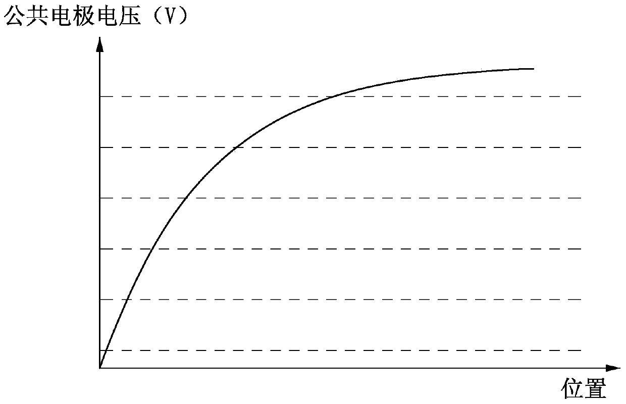
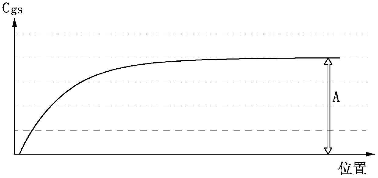
However, in the actual Cgs compensation process, since the feed-through voltage Vp(x) on the pixel electrode decreases sequentially from the signal input end to the end of the scan line, the Cgs corresponding to the signal input end of the scan line is the smallest, and the end corresponds to The Cgs is the largest, and the increasing degree from the signal input end to the end is not a linear increase
Therefore, if the difference in Cgs of transistor elements in adjacent regions is too large, it will cause uneven gray scales in adjacent regions of the panel (such as Figure 5 As shown), regional spots (mura) are formed on the display screen; if the Cgs difference of transistor elements in adjacent regions is too small, then the panel needs to be divided into dozens or even hundreds of parts, so for the actual wiring It is very difficult, increases the workload of wiring, and is not easy to check

Method used


Image

  • Method and array substrate for compensating parasitic capacitance of panel switching element
  • Method and array substrate for compensating parasitic capacitance of panel switching element
  • Method and array substrate for compensating parasitic capacitance of panel switching element

Examples


Embodiment Construction

[0018] In order to further explain the technical means and effects adopted by the present invention to achieve the intended purpose of the invention, the method for compensating the parasitic capacitance of the panel switching element and the array substrate according to the present invention will be discussed below in conjunction with the accompanying drawings and preferred embodiments. Specific embodiments, methods, steps, structures, features and effects are described in detail below.

[0019] The foregoing and other technical contents, features and effects of the present invention will be clearly presented in the following detailed description of preferred embodiments with reference to the drawings. Through the description of specific implementation methods, the technical means and effects of the present invention to achieve the intended purpose can be understood more deeply and specifically, but the accompanying drawings are only for reference and description, and are not ...


PUM


Abstract

The invention provides a method for compensating a stray capacitance of a panel switch element, which comprises the steps that a capacitance value to be compensated for the stray capacitance of the switch element in a pixel unit along different positions of a gate line on a panel is calculated according to the formula C(x)=A(1-e<yx>), wherein C refers to the capacitance value to be compensated, A refers to a differential value between a compensation value of the stray capacitance of the switch element in the pixel unit at a signal input end of the corresponding gate line and a compensation value of the stray capacitance of the switch element in the pixel unit at the tail end of the corresponding gate line, x refers to the position of the pixel unit, and y refers to a constant less than zero; and according to the compensated capacitance, a relative area between two polar plates of the stray capacitances of the switch elements in the pixel units at the different positions along the gate line on the panel is calculated. The invention also provides an array baseplate. The method for compensating the stray capacitance of the panel switch element and the array baseplate provided by the invention realize a steady voltage of a public electrode, require small wiring workloads and realize a good picture display effect.

Description

technical field [0001] The present invention relates to the field of display technology, in particular to a method for compensating parasitic capacitance of panel switching elements and an array substrate. Background technique [0002] Liquid Crystal Display (LCD) has many advantages such as lightness, lightness, energy saving, and no radiation, so it has gradually replaced the traditional cathode ray tube (CRT) display. Currently, liquid crystal display devices are widely used in electronic equipment such as high-definition digital televisions, desktop computers, personal digital assistants (PDAs), notebook computers, mobile phones, and digital cameras. [0003] The liquid crystal display device includes an array substrate, a color filter substrate, and a liquid crystal layer arranged between the array substrate and the color filter substrate. A plurality of insulated and crossed data lines and scan lines are arranged on the array substrate, and each two insulated and cros...

Claims


Application Information

Patent Timeline
Patent Type & Authority Patents(China)
IPC IPC(8): G02F1/1362
CPCG02F1/1362
Inventor 秦刚乔艳冰
Owner KUSN INFOVISION OPTOELECTRONICS
Learn More