Display panel, manufacturing method thereof and display device

A display panel and liquid crystal panel technology, applied in the field of display panels and display devices, can solve the problems of touch sensor signal crosstalk, display panel touch accuracy and sensitivity reduction, etc., to improve accuracy and sensitivity, and reduce signal crosstalk The effect of reducing the effect of parasitic capacitance

CN112415798AActive Publication Date: 2021-02-26SHENZHEN CHINA STAR OPTOELECTRONICS SEMICON DISPLAY TECH CO LTD
6 Cites 1 Cited by

Patent Information

Authority / Receiving Office
CN · China
Patent Type
Applications(China)
Current Assignee / Owner
Publication Date
2021-02-26

Smart Images

  • Figure 1
    Figure 1
  • Figure 2
    Figure 2
  • Figure 3
    Figure 3
Patent Text Reader

Abstract

The invention provides a display panel, a manufacturing method thereof and a display device. The display panel comprises a liquid crystal panel and a touch panel, the touch panel comprises a substrateand a plurality of touch sensors and light-operated sensors, each touch sensor is composed of a plurality of columns of transmitting electrodes and receiving electrodes, and each light-operated sensor comprises a plurality of gate electrodes; the receiving electrodes and the gate electrodes are arranged in a layered manner, and the orthographic projection areas of the plurality of receiving electrodes on the substrate are overlapped with the orthographic projection areas of the gate electrodes on the substrate to form a plurality of overlapping areas. Every two adjacent receiving electrodes,located in each overlapping area, in the same column of receiving electrodes are connected through a conductive electrode arranged on the side, away from a gate electrode, of the receiving electrode,so that parasitic capacitance between the receiving electrodes of the touch sensors and the gate electrodes of the light-operated sensors is reduced, the influence of the light-operated sensors on thesignal crosstalk of the touch sensors is reduced, and the touch accuracy and sensitivity of the display panel integrated with the light-operated sensors and the touch sensors are improved.
Need to check novelty before this filing date? Find Prior Art

Description

technical field

[0001] The present invention relates to the field of display technology, in particular to a display panel, a manufacturing method thereof, and a display device. Background technique

[0002] With the development of display technology, it is also a trend to integrate sensors into display panels. The touch and light sensors currently used are to attach the sensor to the outside of the display panel, which will not only reduce the light transmittance of the display panel, but also increase the manufacturing cost, while integrating the sensor in the display panel can effectively reduce the The loss of light can also reduce manufacturing costs.

[0003] In the existing display panels that synchronously integrate the light control sensor and the touch sensor, the touch sensor is usually a mutual capacitance structure, which is composed of multiple rows of emitting electrodes arranged horizontally and multiple columns of receiving electrodes arranged vertically, an...

Examples

Embodiment Construction

[0032] The following descriptions of the various embodiments refer to the attached drawings to illustrate specific embodiments in which the present application can be practiced. The directional terms mentioned in this application, such as [top], [bottom], [front], [back], [left], [right], [inside], [outside], [side], etc., are for reference only The orientation of the attached schema. Therefore, the directional terms used are used to illustrate and understand the application, but not to limit the application. In the figures, structurally similar elements are denoted by the same reference numerals.

[0033] The present application will be further described below in conjunction with the accompanying drawings and specific embodiments.

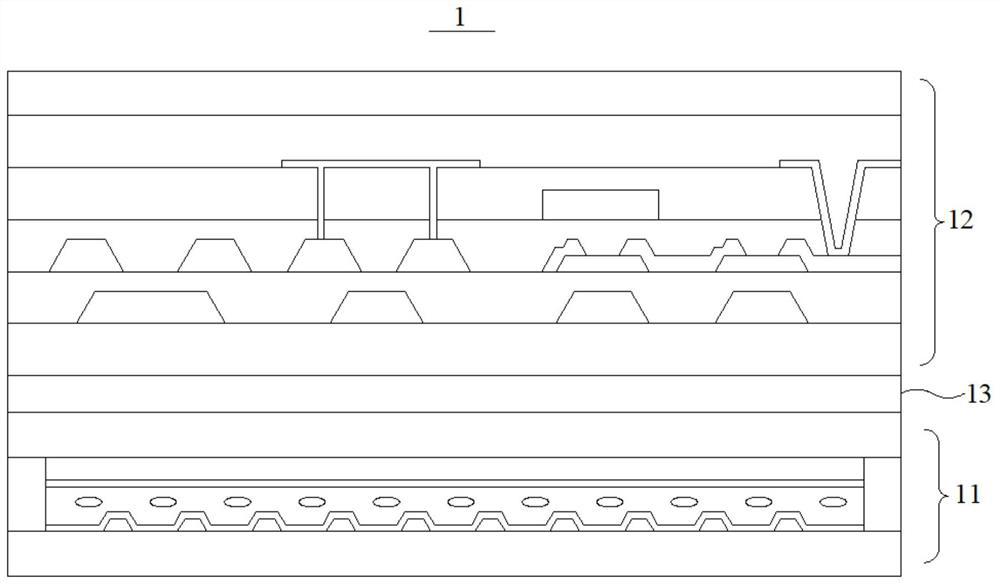
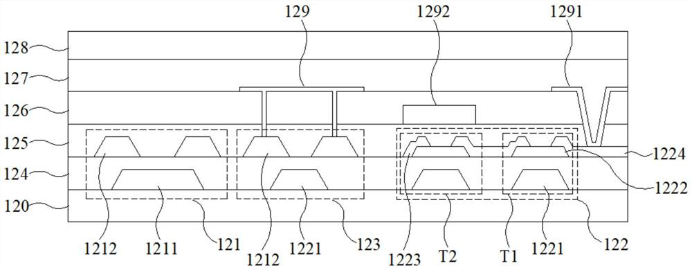
[0034] The embodiment of the present application provides a display panel, which is combined with Figure 1 to Figure 3 For details, figure 1 A schematic structural diagram of a display panel provided in an embodiment of the present applicatio...