Device for transferring charges and display equipment

A technology for transferring charges and charges, applied in circuits, electrical components, electric solid-state devices, etc., can solve problems such as affecting normal display, eliminate the influence of pixel driving current intensity, and solve the effect of color cast on screen display

Pending Publication Date: 2021-09-24
BOE TECH GRP CO LTD +1
View PDF8 Cites 0 Cited by
  • Summary
  • Abstract
  • Description
  • Claims
  • Application Information

AI Technical Summary

Problems solved by technology

[0003] However, after the OLED touch screen is used for a period of time, due to the accum

Method used


Image

  • Device for transferring charges and display equipment
  • Device for transferring charges and display equipment
  • Device for transferring charges and display equipment

Examples


Embodiment Construction

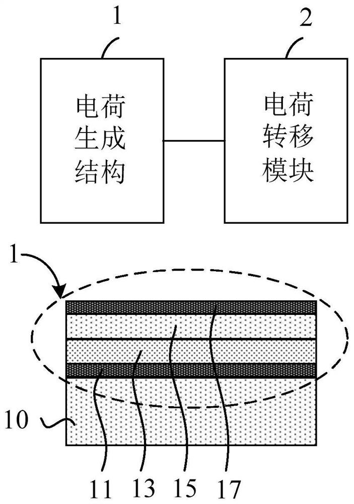
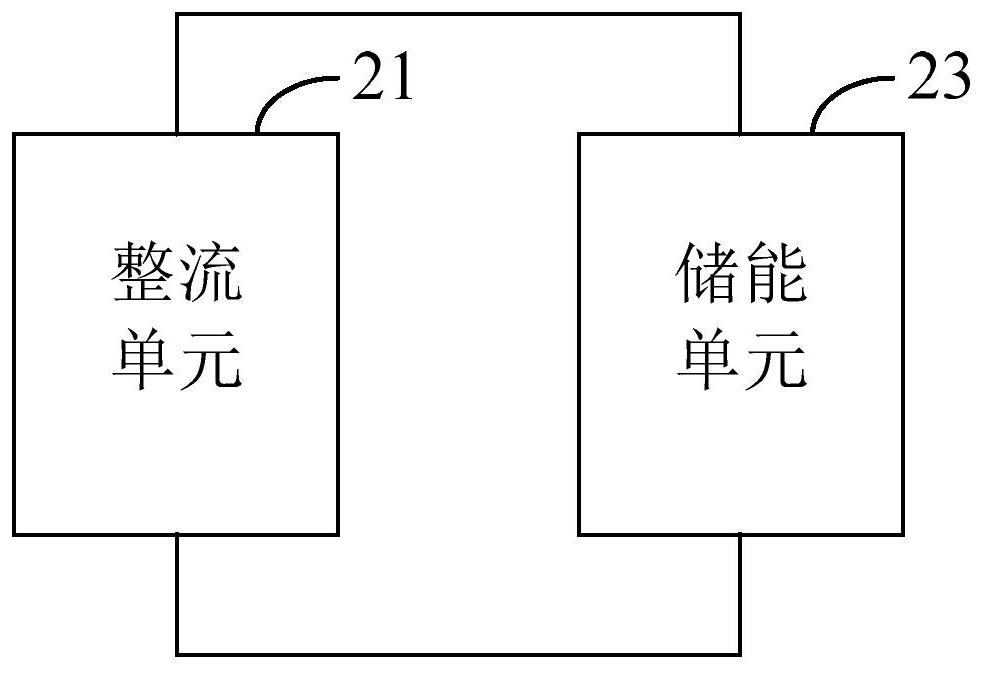
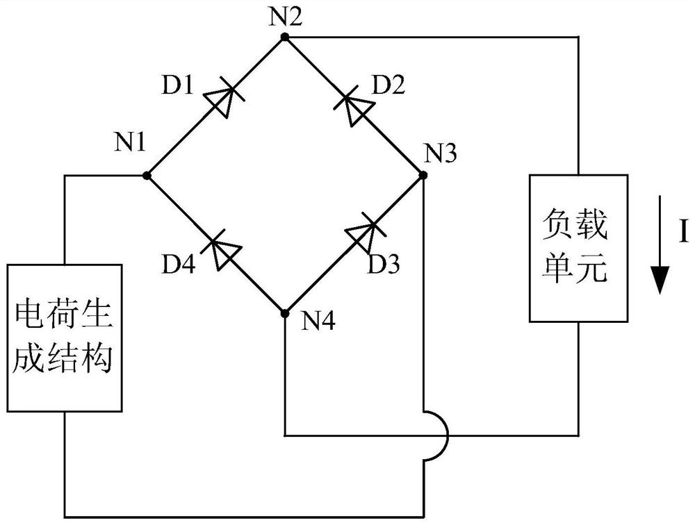
[0019] In order to make the purpose, technical solution and advantages of the present disclosure clearer, the embodiments of the present disclosure will be described in detail below in conjunction with the accompanying drawings. Note that an embodiment may be embodied in many different forms. Those skilled in the art can easily understand the fact that the means and contents can be changed into various forms without departing from the gist and scope of the present disclosure. Therefore, the present disclosure should not be interpreted as being limited only to the contents described in the following embodiments. In the case of no conflict, the embodiments in the present disclosure and the features in the embodiments can be combined arbitrarily with each other.

[0020] In the drawings, the size of each component, the thickness of a layer, or a region is sometimes exaggerated for the sake of clarity. Therefore, one aspect of the present disclosure is not necessarily limited to...


PUM


Abstract

The invention discloses a device for transferring charges. The device comprises a charge generation structure and a charge transfer module; the charge generation structure comprises a first electrode layer, a first dielectric layer, a second dielectric layer and a second electrode layer which are sequentially stacked on the array substrate; the first dielectric layer and the second dielectric layer are oppositely arranged and attached to each other; the first dielectric layer and the second dielectric layer are configured to induce equivalent inductive charges with opposite polarities when deformation is generated or recovered; the first electrode layer is configured to induce equivalent charges with opposite polarities when the first dielectric layer generates the charges; the second electrode layer is configured to induce equivalent charges with opposite polarities when the second dielectric layer generates the charges; and the charge transfer module is configured to transfer inductive charges generated by the charge generation structure on the first electrode layer and the second electrode layer. According to the technical scheme, inductive charges generated when the surface of the screen is affected by external force can be transferred in time, and the situation that normal display is affected due to accumulation of the inductive charges in the panel is avoided.

Description

technical field [0001] This article relates to but not limited to the field of display technology, and in particular relates to a device for transferring charges and a display device. Background technique [0002] With the development of display technology, OLED (Organic Light-Emitting Diode, Organic Light-Emitting Diode) products have achieved rapid development due to many advantages such as self-illumination, high brightness, and wide viewing angle. [0003] However, after the OLED touch screen is used for a period of time, the normal display may be affected due to the accumulation of induced charges generated during the touch in the device. Contents of the invention [0004] In a first aspect, the present disclosure provides a device for transferring charges, including: a charge generating structure arranged in the display area of ​​the display panel and a charge transfer module arranged outside the display area of ​​the display panel; [0005] The charge generation st...

Claims


Application Information

Patent Timeline
IPC IPC(8): H01L51/52H01L27/32
CPCH10K59/40H10K59/12H10K50/80Y02B40/00
Inventor 陈佳高栋雨刘刚虎李会会聂汉邓成绩李鑫赵根仝勋飞
Owner BOE TECH GRP CO LTD
Why Eureka
Try Eureka