A method for manufacturing a chip oxygen sensor chip
An oxygen sensor and manufacturing method technology, applied in instruments, scientific instruments, measuring devices, etc., can solve the problems of easy introduction of impurities, high cost, poor performance, etc., and achieve enhanced heat transfer effect, reduced production cost, and simple process flow. Effect
- Summary
- Abstract
- Description
- Claims
- Application Information
AI Technical Summary
Problems solved by technology
Method used
Image
Examples
Embodiment 1
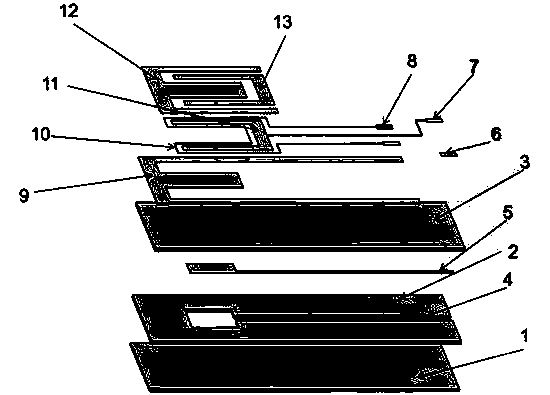
[0028] Such as figure 1 , figure 2 As shown, the structure of the oxygen sensor chip is an upper functional sheet (abbreviated as the upper sheet 3), a middle channel forming sheet (abbreviated as the middle sheet 2) and a lower layer sheet (abbreviated as the lower sheet 1), which are sequentially stacked and hot-pressed to form a whole. Its manufacturing process steps include: A. Preparation of casting slurry: adding 1.5% dispersant triethanolamine, 10% Adhesive polyvinyl butyral, 5% plasticizer butyl benzyl phthalate and 5% lubricant polyethylene glycol are made into cast slurry in an organic solvent by ball milling; B , Casting: Scrape the casting slurry on the casting machine with a scraper on the backing belt to form a film of uniform thickness, and remove the film after drying; C. Lamination punching: Laminate the upper, middle and lower blanks of the designed thickness, Make positioning holes and process holes with a punching machine respectively; D, printing: print...
Embodiment 2
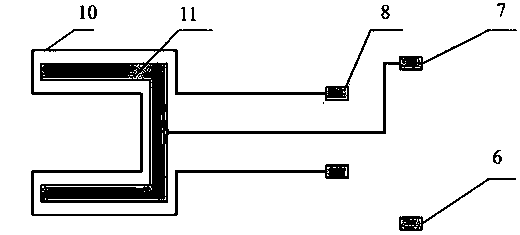
[0030] The structure of the oxygen sensor chip is simplified as an upper layer functional sheet and a lower layer sheet, which are sequentially stacked and hot-pressed to form a whole. The process steps are the same as in Example 1. The design of the upper layer functional sheet is as follows: image 3 As shown, the printing steps are: printing and coating the internal electrode 5 and the external electrode 11 on the upper sheet 3, printing the protective layer 13 on the working area of the external electrode 11, printing and coating the insulating layer 9, The heating resistor 10 and the cover layer 12, the inner electrode 5 is connected to the pin 6 of the outer layer through a small hole, the outer electrode is connected to the outer electrode pin 7 through a lead wire, and the heating resistor is connected to the heating resistor pin 8 through a lead wire; The air channel 4 is formed by upper printing.
[0031] All the other are identical with embodiment 1.
PUM
 Abstract
Description
Claims
Application Information


