Novel replaceable single-layer metal layout structure of TVS

A layout structure and metal technology, applied in the direction of electrical components, electrical solid devices, circuits, etc., can solve the problems of occupying a large area and reducing the wiring area of ​​the circuit board, and achieve uniform distribution of current, good quality and performance, and reduced The effect of possible errors

Pending Publication Date: 2021-10-22
电子科技大学重庆微电子产业技术研究院
View PDF6 Cites 0 Cited by
  • Summary
  • Abstract
  • Description
  • Claims
  • Application Information

AI Technical Summary

Problems solved by technology

[0004] At the same time, there are often multiple pins on the circuit board that have electrostatic risks. In order to effectively protect multiple pins, it is necessary to protect multiple pins at the same time. If a single-channel devic

Method used


Image

  • Novel replaceable single-layer metal layout structure of TVS
  • Novel replaceable single-layer metal layout structure of TVS
  • Novel replaceable single-layer metal layout structure of TVS

Examples


Example Embodiment

[0023] Example 1

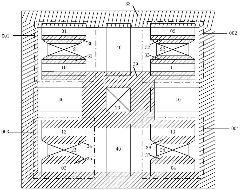
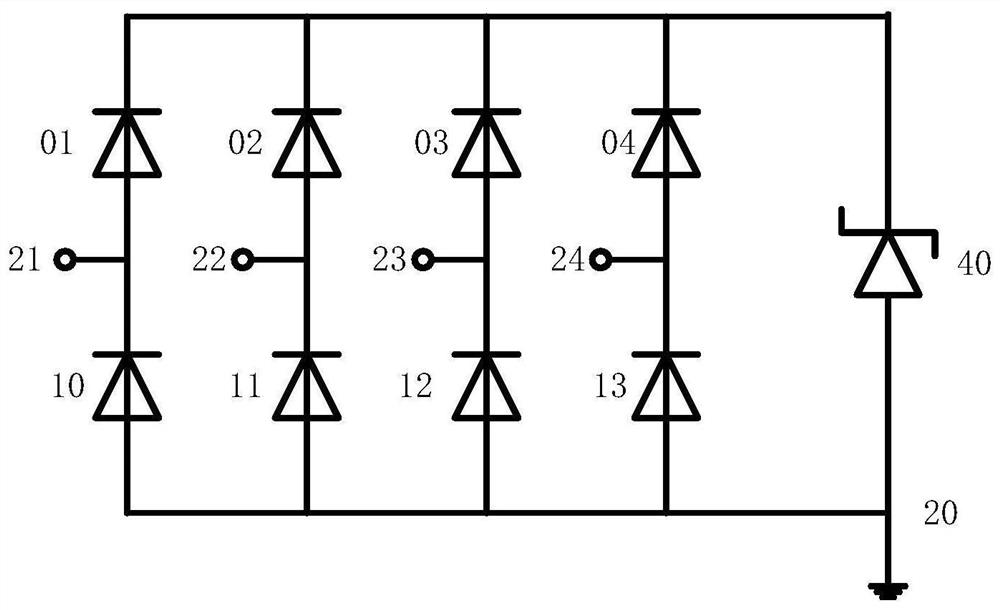
[0024] like figure 1 As shown, this embodiment provides a novel alternative TVS single-layer metal layout structure, including: a first diode 01, a second diode 02, a third diode 03, and a fourth diode 04 , the fifth diode 10, the sixth diode 11, the seventh diode 12, the eighth diode 13, the zener tube 40; the first electrode pad 20, the second electrode pad 21, the third Electrode pad 22, fourth electrode pad 23, fifth electrode pad 24; first metal 30, second metal 31, third metal 32, fourth metal 33, fifth metal 34, sixth metal 35, The seventh metal 36, the eighth metal 37, the ninth metal 38, and the tenth metal 39;

[0025] Among them, the first diode 01, the fifth diode 10, the second electrode pad 21, the first metal 30 and the second metal 31 form the first diode region 001, and the first diode region 001 is located in the layout The upper left corner of the structure; wherein the second electrode pad 21 is connected to the p-region of the first d...

Example Embodiment

[0031] Example 2

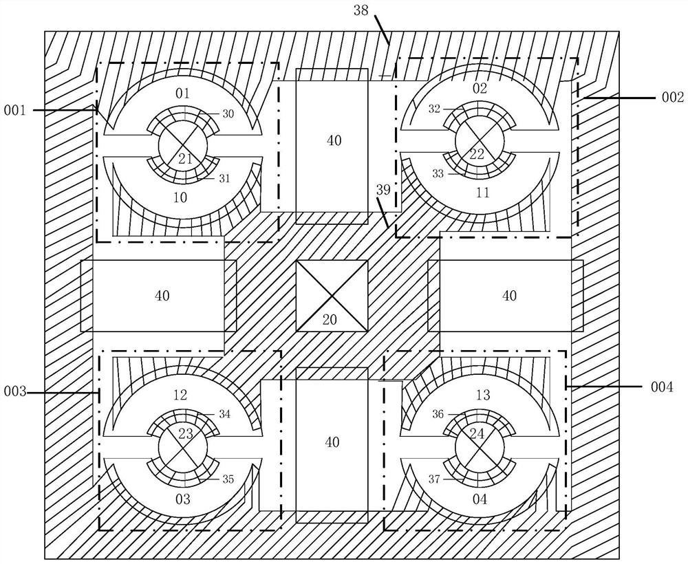
[0032] like image 3 As shown, the difference between this embodiment and Embodiment 1 is: the first diode 01, the second diode 02, the third diode 03, the fourth diode 04, the fifth diode 10, the first diode The six diodes 11, the seventh diode 12, and the eighth diode 13 are circular, and the second electrode pad 21, the third electrode pad 22, the fourth electrode pad 23, and the fifth electrode pad 24 is round.

Example Embodiment

[0033] Example 3

[0034] The difference between this embodiment and Embodiment 1 is that the Zener transistor 40 is a thyristor.


PUM


Abstract

The invention provides a novel replaceable single-layer metal layout structure of a TVS. In a low-capacitance guide diode type TVS array or a multi-channel multi-pin ESD protection design, according to the layout, all modules are reasonably arranged in corresponding areas, a complete signal path is formed through single-layer metal connection, a low-cost single-layer metal layout structure is achieved, meanwhile, current distribution is optimized, the layout area is reduced, and meanwhile, the production cost of the chip is reduced, and the robustness of the device is improved.

Description

technical field [0001] The invention belongs to the field of electronic science and technology, and is mainly used for the protection technology of Electro Static Discharge (ESD for short). Specifically, it refers to a new replaceable single-layer metal layout structure of TVS. Background technique [0002] Electrostatic discharge ESD (Electro-static discharge, electrostatic discharge) is ubiquitous in the process of chip manufacturing, packaging, testing and use. When released, the instantaneous power can reach hundreds of kilowatts, and the discharge energy can reach millijoules, which can destroy the chip extremely strongly. According to statistics, more than 35% of chip failures are caused by ESD damage. Therefore, the design of electrostatic protection module in chip design is directly related to the functional stability of the chip, which is extremely important. [0003] Since it is difficult to reduce the capacitance of a single TVS tube, while the working voltage a...

Claims


Application Information

Patent Timeline
IPC IPC(8): H01L23/60H01L27/02
CPCH01L23/60H01L27/0292
Inventor 齐钊刘超牛中乾李泽宏唐鹤张波
Owner 电子科技大学重庆微电子产业技术研究院
Why Eureka
Try Eureka