Pin bending device of silicon carbide diode

A technology of silicon carbide diodes and bending devices, applied in the field of diodes, can solve problems such as reducing work efficiency, not controlling the bending distance of pins, and deformation of diode pins

Active Publication Date: 2022-02-01
先之科半导体科技(东莞)有限公司
View PDF10 Cites 9 Cited by
  • Summary
  • Abstract
  • Description
  • Claims
  • Application Information

AI Technical Summary

Problems solved by technology

[0003] The existing diode pin bending device, such as a diode bending machine disclosed in patent number CN202022706009.8, can easily bend the diode through the fixing device and pressing device at both ends, but it needs to be manually bent. To place or take out the diode, at the same time, because its fixed component cannot be moved, it does not know the bending distance required by the control pin, which greatly reduces its working efficiency, and it may also be possible to place or take out the diode because of the bracket at its upper end. When a collision occurs, the diode pins are deformed, which increases the cost

Method used


Image

  • Pin bending device of silicon carbide diode
  • Pin bending device of silicon carbide diode
  • Pin bending device of silicon carbide diode

Examples


Embodiment Construction

[0044] In order to further understand the features, technical means, and specific objectives and functions achieved by the present invention, the present invention will be further described in detail below in conjunction with the accompanying drawings and specific embodiments.

[0045] Such as Figure 1-10 As shown, this application provides:

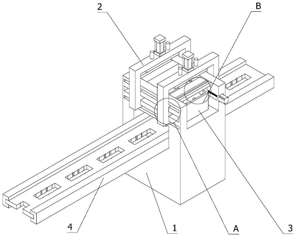
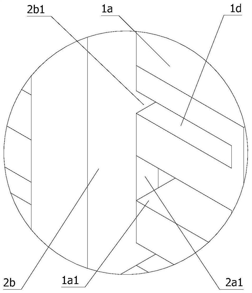
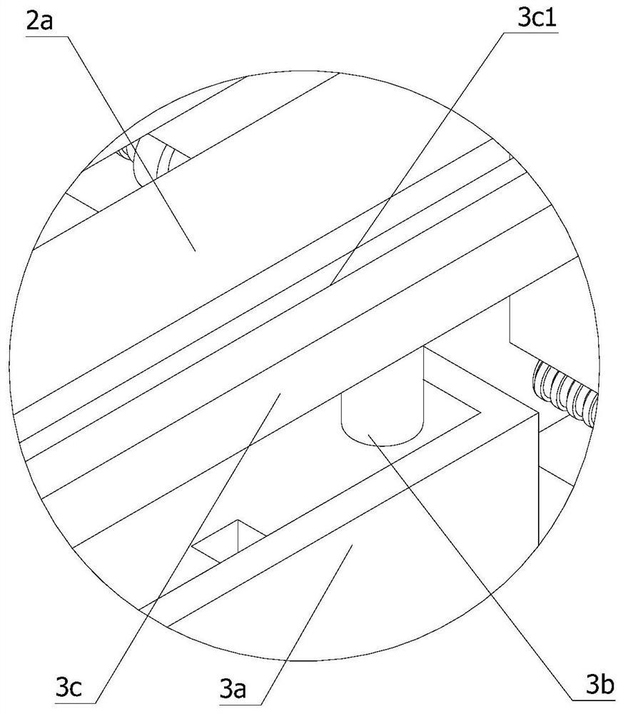
[0046] A pin bending device for a silicon carbide diode, comprising a workbench 1, a fixing assembly 2, and a bending assembly 3, the top of the workbench 1 is provided with two evenly distributed first brackets 1a; the fixing assembly 2 is provided with two and All can be movable on the first bracket 1a; the bending assembly 3 is arranged on the fixed assembly 2; the workbench 1 is also provided with a transmission assembly for transmitting diodes, and the transmission assembly includes a first conveyor 4, a first push plate 5 and the first linear drive 6, the first conveyor 4 is partially pierced on the workbench 1, and the transmiss...


PUM


Abstract

The invention relates to the technical field of diodes, in particular to apin bending device of a silicon carbide diode. The pin bending device comprises a workbench, a fixing assembly and a bending assembly. The workbench is further provided with a transmission assembly used for transmitting diodes. The transmission assembly comprises a first transmission machine, a first push plate and a first linear driver. According to the pin bending device of the silicon carbide diode, the diode is placed in a groove in the first transmission machine, the diode is transmitted along with the transmission face of the first transmission machine, the first transmission machine is controlled to stop or operate through external detection equipment, and the diode reaches the designated position; then, a first push plate is pushed upwards through a first linear driver, the first push plate penetrates through a groove corresponding to the first push plate, so that the diode on the groove is driven to move upwards to a fixing assembly to be fixed, a bending assembly is bent, and then the diode is driven by the first linear driver to return to the conveying surface; and the problem that an existing diode is low in the corner folding efficiency is solved.

Description

technical field [0001] The invention relates to the technical field of diodes, in particular to a pin bending device for silicon carbide diodes. Background technique [0002] Diode refers to a device with two electrodes that only allows current to flow in a single direction. Many uses are for its rectification function, while varactor diodes are used as electronic adjustable capacitors. Most diodes The current directionality we have is usually called the "rectification" function. The most common function of a diode is to only allow current to pass in a single direction and block it when it is reversed. Therefore, a diode can be thought of as an electronic version of a check valve. When the diode is installed, its pins need to be bent first, and the pins can only be installed on the circuit board after the pins are bent. [0003] The existing diode pin bending device, such as a diode bending machine disclosed in patent number CN202022706009.8, can easily bend the diode throu...

Claims


Application Information

Patent Timeline
Patent Type & Authority Applications(China)
IPC IPC(8): B21F1/00B21F23/00H01L21/67H01L21/677
CPCB21F1/00B21F23/005H01L21/67138H01L21/67742
Inventor 周勇
Owner 先之科半导体科技(东莞)有限公司
Why Eureka
Try Eureka