Active matrix display device

A display device and active matrix technology, applied in static indicators, nonlinear optics, instruments, etc., can solve problems such as display device malfunction and achieve the effect of preventing malfunction

CN1264126CInactive Publication Date: 2006-07-12SANYO ELECTRIC CO LTD
1 Cites 0 Cited by

Patent Information

Authority / Receiving Office
CN · China
Current Assignee / Owner
Publication Date
2006-07-12
Estimated Expiration
Not applicable · inactive patent

Smart Images

  • Figure 1
    Figure 1
  • Figure 2
    Figure 2
  • Figure 3
    Figure 3
Patent Text Reader

Abstract

The invention aims to secure the operation of an active matrix type display device with a holding circuit. The holding circuit 110 for holding a video signal every pixel is arranged, and a normal operation mode and a memory operation mode are switched to each other for displaying. In the memory operation mode, a gate signal line 51 or / and a drain signal line 61 are fixed at a prescribed voltage. Therefore, a transistor connected with the gate signal line 51 or / and the drain signal line 61 can be prevented from operating erroneously. Grounding transistors 401, 402 connected with the gate signal line 51 or / and the drain signal line 61 are realized to be switched on in the memory operation mode.
Need to check novelty before this filing date? Find Prior Art

Description

technical field

[0001] The present invention relates to an active matrix display device, and more particularly to an active matrix display device provided with a plurality of holding circuits corresponding to pixels. Background technique

[0002] In recent years, as a market demand, display devices are required to be portable, such as portable televisions, mobile phones, and the like. In response to such demands, research and development for miniaturization, weight reduction, and power saving of display devices has been actively conducted. Japanese Unexamined Patent Publication No. 2000-282168 discloses a liquid crystal display device in which a static random access memory (SRAM) is provided in each display pixel to display a still image.

[0003] Figure 5 A circuit configuration diagram of a conventional liquid crystal display device (Liquid Crystal Display; LCD) is shown. In the liquid crystal display device 100 , a plurality of pixel electrodes 17 are arranged in a mat...

Examples

Embodiment Construction

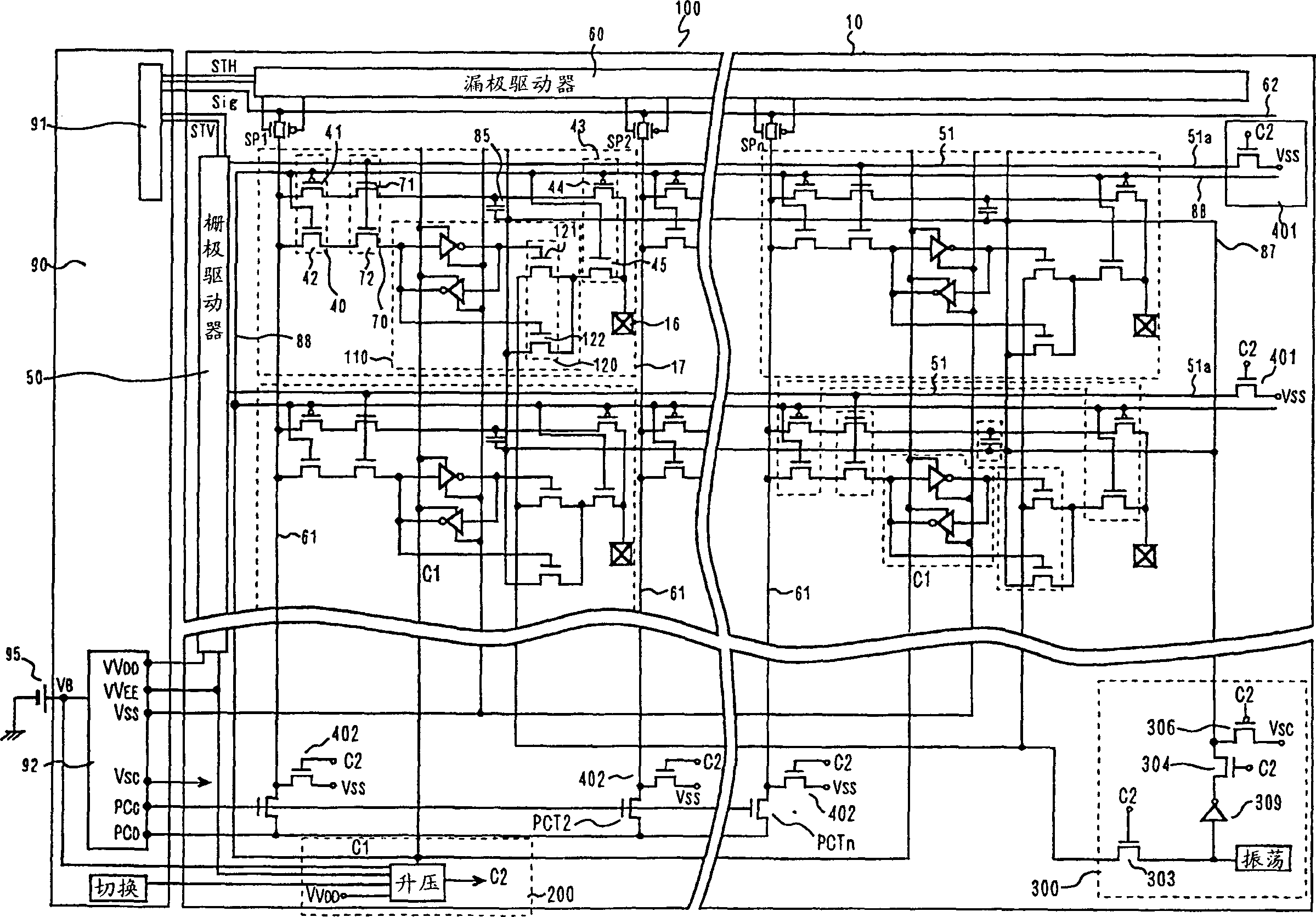
[0045] A display device according to an embodiment of the present invention will now be described. figure 1 A circuit configuration diagram when the display device of the present invention is applied to a liquid crystal display device is shown in . The pixel portion of the display device of this embodiment is substantially the same as the conventional one. That is, in this embodiment, the analog operation circuit having the selection TFT 71 and the auxiliary capacitor 85 and the storage operation circuit having the holding circuit 110 are switched by the circuit selection circuits 40 and 43 to switch between the normal operation mode and the storage operation mode and display. The same symbols are assigned to the same structures as conventional ones, and detailed description thereof will be omitted.

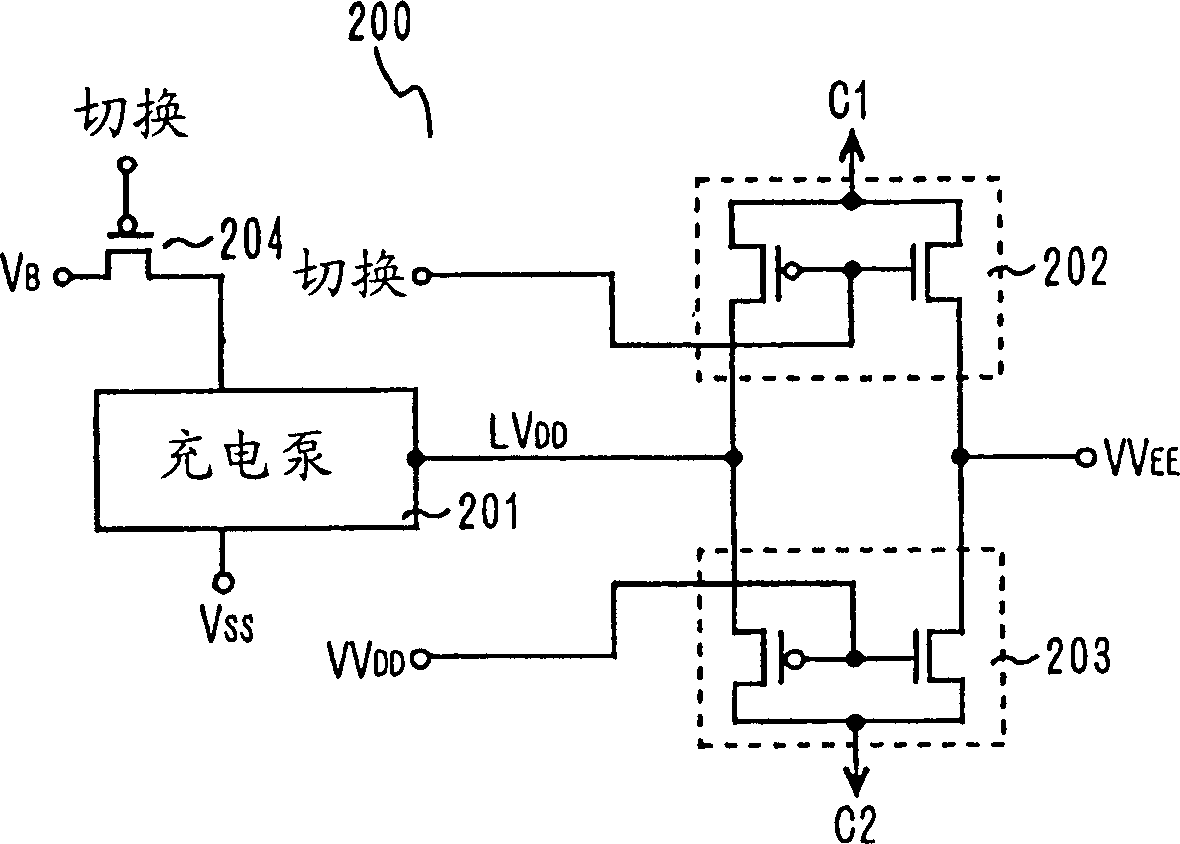
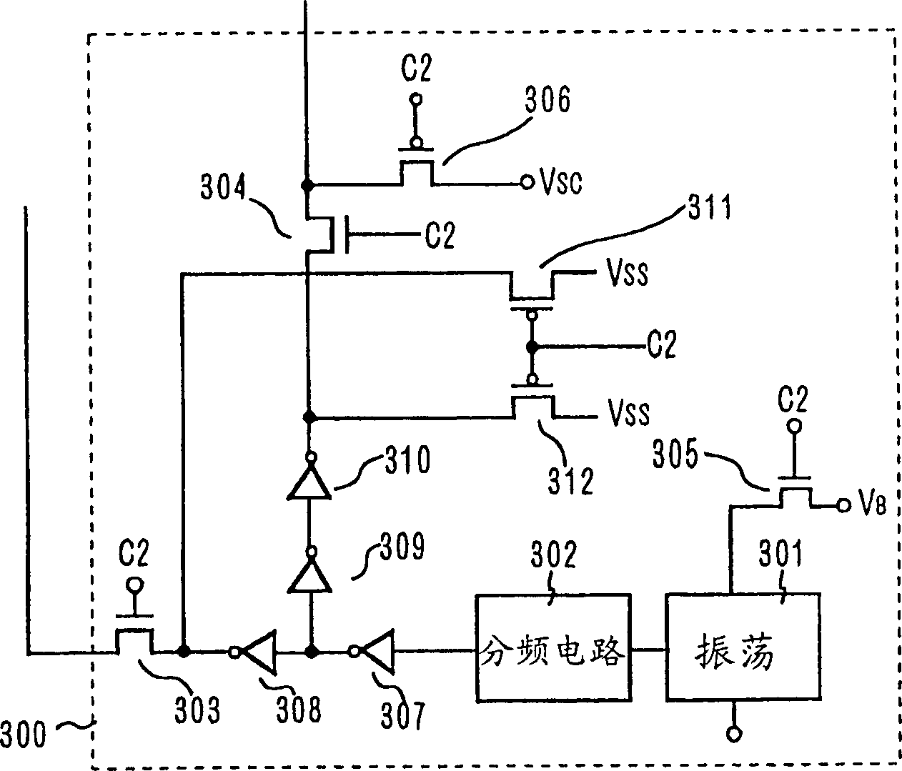
[0046] The display device of this embodiment has a booster circuit 200, an oscillation unit 300, a ground switch 401, and a ground switch 402 inside the LCD panel 100, which is...