D/A converter and conversion method with compensation to reduce clock jitter

A technology of analog converter and analog conversion, which is applied in the direction of digital-to-analog converter, analog-to-digital converter, and data exchange through path configuration, which can solve the problems of complex design of analog front-end circuits

A technology of analog converter and analog conversion, which is applied in the direction of digital-to-analog converter, analog-to-digital converter, and data exchange through path configuration, which can solve the problems of complex design of analog front-end circuits

CN1433189AInactive Publication Date: 2003-07-30SILICON INTEGRATED SYSTEMS

Image

  • D/A converter and conversion method with compensation to reduce clock jitter
  • D/A converter and conversion method with compensation to reduce clock jitter
  • D/A converter and conversion method with compensation to reduce clock jitter

Examples


Embodiment Construction

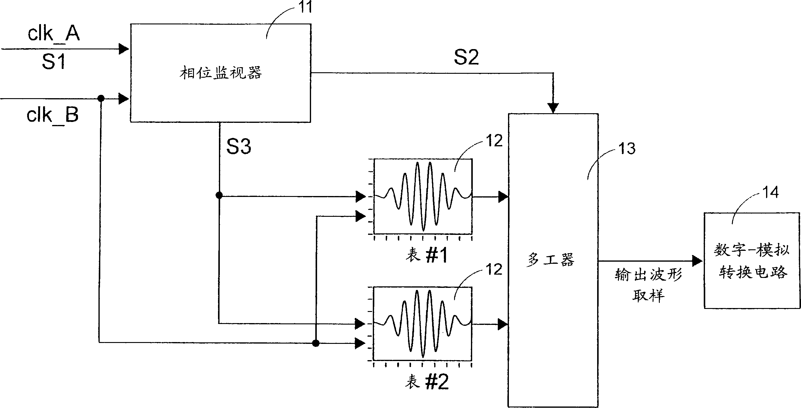
[0023] When a digital-to-analog converter is used in a common digital transmission system to convert data from a digital format to an analog format, the frequency of the driving (digital-to-analog conversion) clock is usually the same as the system clock or an integer multiple of the system clock, otherwise, When the transmission continues, the transmitted waveform pulse will gradually deviate from the ideal timing. In addition to the jitter of the system clock itself, the jitter of the transmitted waveform is added. This jitter is caused by the difference between the system clock and the digital-to-analog conversion clock. The frequency difference is the so-called out-of-sync, and the maximum value of jitter can usually be as large as one digital-to-analog conversion period. Now we use figure 1 Describe how to reduce the jitter of the system according to the present invention.

[0024] We assume that the period of the system clock clk-A is T A , while the period of the digit...


PUM


Abstract

A digital-analog conversion method which can decrease jitter phenomenon when operation is carried on with two clock messages in different preriod includes the following steps: monitoring phase relation between two clock messages: starting transmission of multiset of wave form sampling stored in advance corresponding to each rising wave range of the first clock message and there will be a phase difference existing between any two sets of wave form sampling; exporting wave form sampling for each set corresponding to rising wave range of the second clock message and convertnig one set selected out from multiset of wave form sampling stored in advance according to phase relation into analog message. A digital-analog converter is composed of phase monitor, multiple wave form sampling mater, multiplexer and a digital-analog conversion circuit.

Description

technical field [0001] The present invention relates to a digital-to-analog converter (digital-to-analog converter, DAC) and its conversion method, especially to a digital-to-analog converter and its conversion method operated under two clock signals with different periods, such as Said that this digital-to-analog converter and conversion method can be used in Home PNA 1.0 / 2.0 compatible modules or other digital transmission systems that use pre-synthesized waveforms as the source of transmission signals, and the phenomenon of clock jitter can be improved. Effect. Background technique [0002] Clock jitter has always been a very important problem in the transmission system. If there is a large clock jitter when transmitting signals, it will seriously affect the performance of the system. For example, in the international home network standard HomePNA 1.0, the signal carrying information will be Transmission and processing in sequence (information is...

Claims


Application Information

Patent Timeline
30 Jul 2003
Publication
CN1433189A
IPC
H03M1/12; H03M1/66; H04L12/28
Inventors
曾扬钟; 邹庆锴