
Pushbutton structure

A button and keycap technology, applied in the field of button structure, can solve problems such as wrong signal input

Inactive Publication Date: 2004-05-05
DARFON ELECTRONICS CORP
View PDF0 Cites 2 Cited by
  • Summary
  • Abstract
  • Description
  • Claims
  • Application Information

AI Technical Summary

Problems solved by technology

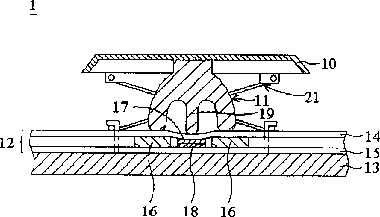
Therefore, if Figure 4 As shown, when the film assembly 12 is arranged on the substrate 13, the second film 15 of the film assembly 12 will protrude due to the above-mentioned foreign matter 20. It is spaced apart from the second conduction portion 18, so when the key structure 1 is not touched, the first conduction portion 17 will improperly contact the second conduction portion 18, thus causing wrong signal input

Method used


Image

  • Pushbutton structure
  • Pushbutton structure
  • Pushbutton structure

Examples


no. 1 example

[0028] see Figure 5 , The button structure 100 of the present invention mainly includes a keycap 110 , an elastic body 120 , a film assembly 130 , a substrate 140 and a connection mechanism 145 . The elastic body 120 is connected to the keycap 110 and disposed under the keycap 110 . The film assembly 130 is disposed under the elastic body 120 . The substrate 140 is disposed under the membrane assembly 130 . One end of the connecting mechanism 145 is connected to the substrate 140 , and the other end of the connecting mechanism 145 is connected to the keycap 110 . The keycap 110 is connected to the base plate 140 in a manner that can move up and down through the connecting mechanism 145 .

[0029] The film assembly 130 has a first film 150 , a second film 160 and a spacer 170 . A first conduction portion 180 and a second conduction portion 190 are respectively provided on the opposite surfaces of the first film 150 and the second film 160, and the first conduction portion ...

no. 2 example

[0033] see Image 6 The difference between this embodiment and the first embodiment is only that the foreign object removal portion 210 of the substrate 140 is a concave portion, and the structure and arrangement of the other key structure 100 components are the same as those of the first embodiment, so no further description is given.

[0034] Likewise, when foreign matter such as dust or sand exists on the substrate 140 , the foreign matter may fall into the concave portion 210 . Therefore, when the film assembly 130 is disposed on the substrate 140, the second film 160 will not protrude due to foreign matter on the substrate 140, and furthermore, the second film 160 will not be raised when the button structure 100 is not touched. Improper electrical connection occurs between the first conducting portion 180 of a thin film 150 and the second conducting portion 190 of the second thin film 160 .

no. 3 example

[0036] see Figure 7 , the button structure 300 of this embodiment is a button structure of a mobile phone. The difference between this embodiment and the first and second embodiments is that the structure of the keycap 110' of the key structure 300 is different from that of the keycap 110 of the key structure 100. At the same time, the key structure 300 does not have a connection mechanism, that is, the keycap 110' is not connected to the substrate 140 in a manner that can move up and down through the connection mechanism, so the up and down movement of the keycap 110' is directly conduct. In addition, the structure and configuration of the remaining components of the key structure 300 are the same as those in the first embodiment, so details are not repeated here.

[0037] Likewise, when foreign matter such as dust or sand exists on the substrate 140 , the foreign matter can be discharged through the through hole 200 . Therefore, when the film assembly 130 is disposed on ...


PUM


Abstract

A key structure is composed of a key cap, an elastic body under said key cap, a thin film assemblage under said elastic body and consisting of the first and the second films and a spacer between them, and a base board, under the thin film assemblage and with a foreign substance rejecting part for rejecting the foreign substance from the base board.

Description

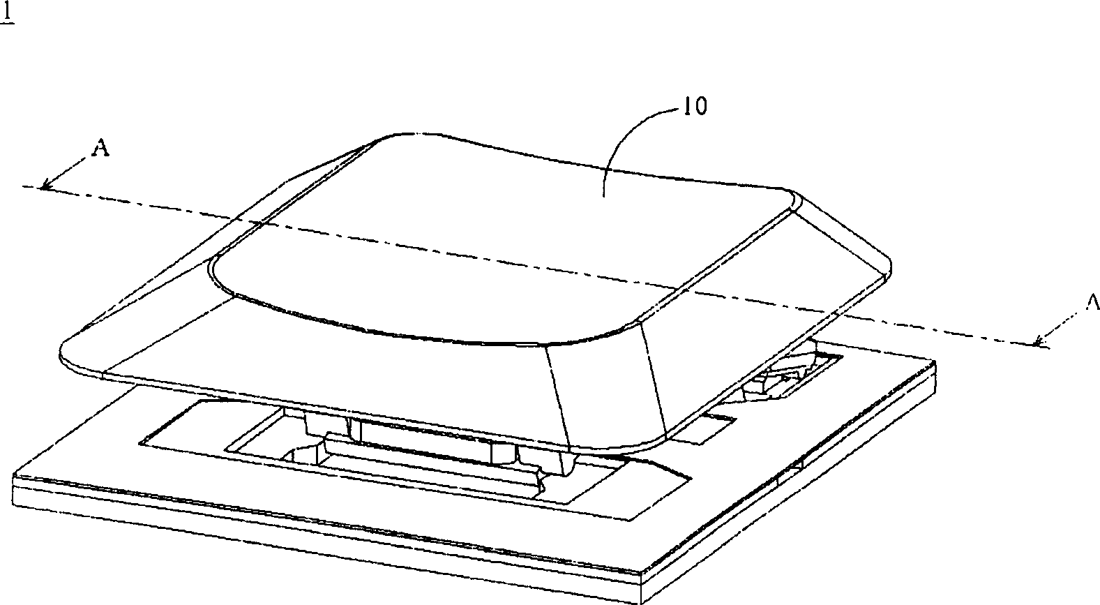
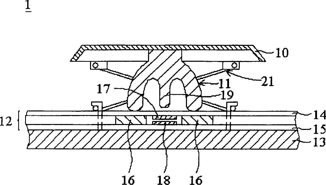
technical field [0001] The invention relates to a key structure, in particular to a key structure capable of removing foreign matter on a substrate without causing wrong signal input. Background technique [0002] figure 1 It is an existing button structure 1 . figure 2 It is a schematic sectional view of A-A showing the existing key structure 1 . Generally speaking, the existing key structure 1 is arranged on a keyboard of a notebook computer as a signal input device. Meanwhile, the key structure 1 is mainly composed of a key cap 10 , an elastic body 11 , a film assembly 12 , a substrate 13 and a connecting mechanism 21 . The elastic body 11 is connected to the keycap 10 and disposed under the keycap 10 . The film assembly 12 is disposed under the elastic body 11 and has a first film 14 , a second film 15 and a spacer 16 . The spacer component 16 is disposed between the first film 14 and the second film 15 . Meanwhile, the membrane assembly 12 is disposed on the subs...

Claims


Application Information

Patent Timeline
Patent Type & Authority Applications(China)
IPC IPC(8): G06F3/02
Inventor 赵世宏
Owner DARFON ELECTRONICS CORP
Learn More