Method for producing transparent conductive film

A technology of transparent conductivity and transparent conductive film, which is applied in the direction of cable/conductor manufacturing, conductive layer on insulating carrier, circuit, etc., can solve the problems such as bubbles and deformation of transparent conductive film, so as not to reduce the display quality, The effect of suppressing the number of scratches

Inactive Publication Date: 2005-05-18
NITTO DENKO CORP
View PDF1 Cites 10 Cited by
  • Summary
  • Abstract
  • Description
  • Claims
  • Application Information

AI Technical Summary

Problems solved by technology

[0006] However, in the above-mentioned manufacturing process of the previous transparent conductive film, at least one surface of the hard-coated film before lamination and the conductive film has unevenness caused by scratches, and the transparent conductive film after lamination is easy. Bubbles or deformation

Method used


Image

  • Method for producing transparent conductive film
  • Method for producing transparent conductive film
  • Method for producing transparent conductive film

Examples


Embodiment 1

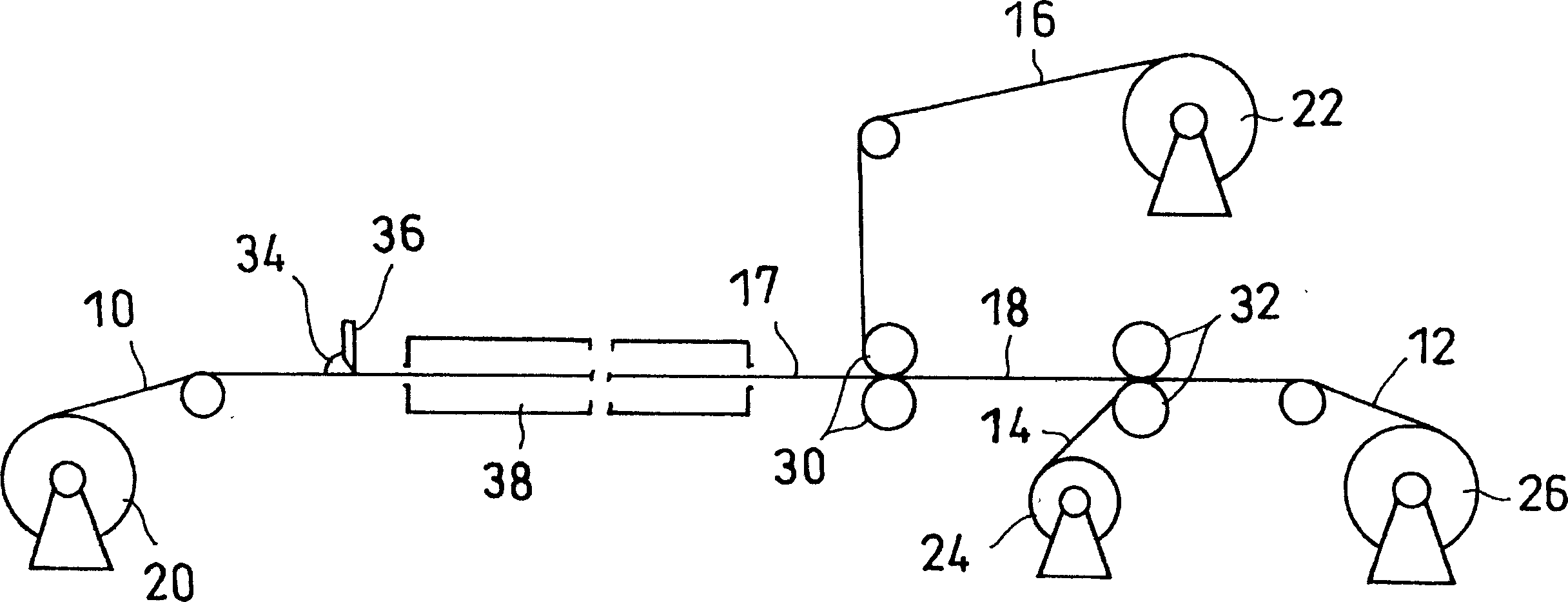
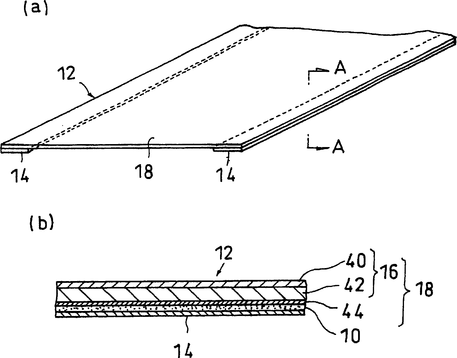
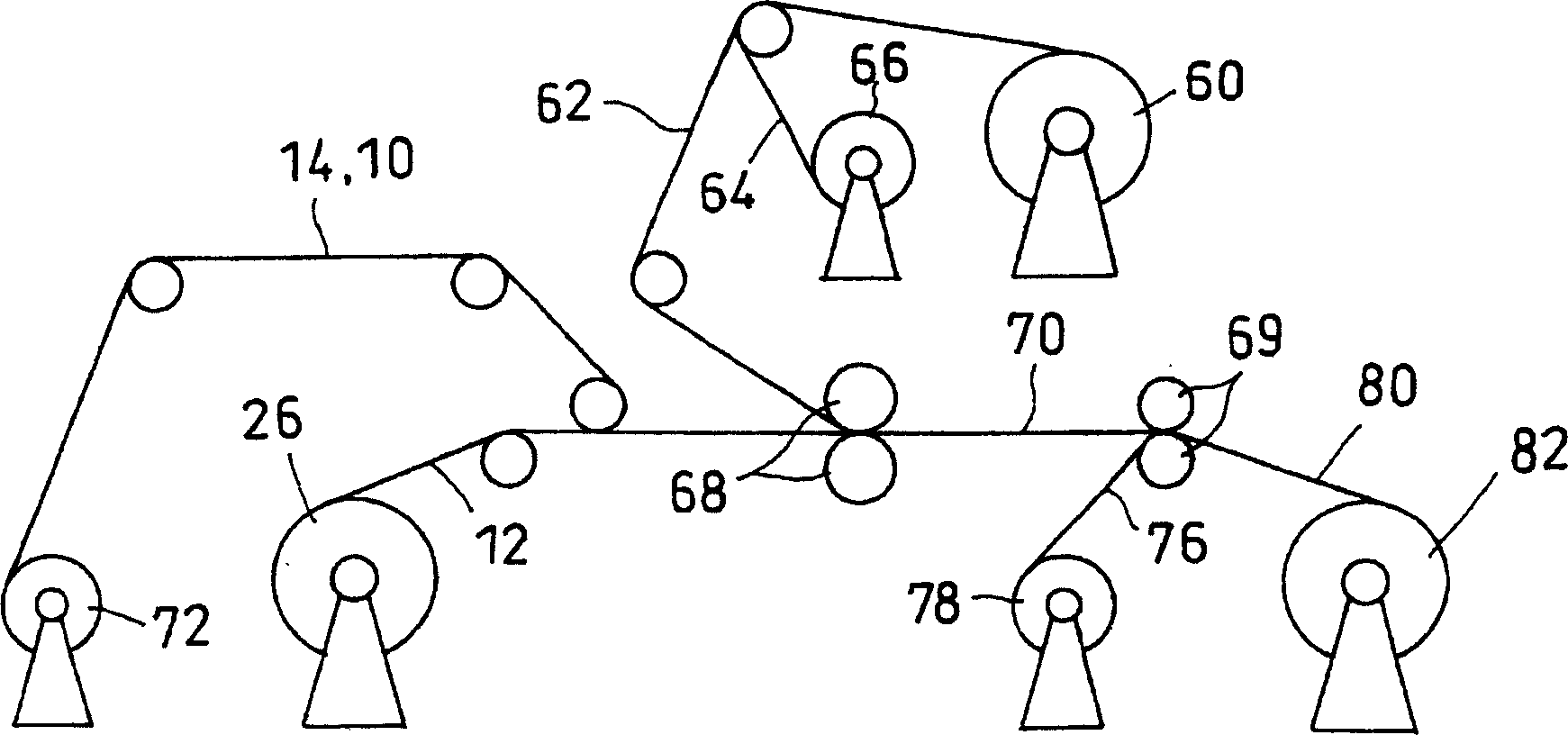
[0053] An HC film (first film) having a 5-μm-thick hard-coat treatment layer made of acrylic urethane resin on the first surface of a 125-μm-thick PET film (first substrate) was obtained.

[0054] An acrylic adhesive layer with a thickness of 25 μm was formed on a spacer with a thickness of 38 μm using a spray-type coater, and adhered to the first base material of the first film, that is, the PET film without a hard coat treatment layer. On the surface (second surface), it is used as an HC film adhesive product (the first film with an adhesive layer). A polyolefin-based co-extruded protective film with a 20mm wide adhesive layer is inserted into both ends of the HC film adhesive in such a way that it adheres to the spacer (adhesion force: 30mN based on JIS-Z-1552 / 25mm), take up HC film adhesive products.

[0055] Form an ITO film (second film) by forming an ITO vapor-deposited film on the first surface of a PET film (second substrate) with a thickness of 23 μm, and insert a ...


PUM


Abstract

The present invention provides a method for producing a transparent conductive film for a touch panel that suppresses unevenness due to scratches, does not cause dents or deformation of images, and does not degrade display quality when used as a display. It is a kind of transparent conductive film ( 70) A manufacturing method comprising: providing spacers at both ends between the second surface of the spacer (10) of the first film (18) with an adhesive layer and the first film (16), and The process of simultaneously winding on a core to form a roll body of the first film with an adhesive layer, removing the spacer (10) while unwinding from the roll body of the first film (18) with an adhesive layer And a lamination process in which the second film (62) is supplied and adhered from the roll body wound on the core through the liner at both ends.

Description

technical field [0001] The present invention relates to a method of manufacturing a transparent conductive film having a hard coat layer and / or an antiglare layer, and more particularly to a method of manufacturing a transparent conductive film suitable for electrode plates of analog touch panels. Background technique [0002] Thin-film resistive touch panels are often used in liquid crystal displays, and as transparent conductive films used for such touch panels, it is known to form a hard coat layer on the first surface of a first transparent base material using an adhesive. A transparent conductive film in which a hard-coat treated film and a conductive film having a transparent conductive film on the first surface of a second transparent substrate are laminated so that their second surfaces face each other (see Patent Document 1). [0003] This transparent conductive film is formed by forming an adhesive layer on one surface of a hard coat-treated film or a conductive fi...

Claims


Application Information

Patent Timeline
Patent Type & Authority Applications(China)
IPC IPC(8): B65H39/16B29C65/48B29D7/01B29L9/00B29L11/00B32B7/02G06F3/033G06F3/041H01B5/14H01B13/00
CPCB29C65/52B29C66/83413B29D7/01B32B7/02B65H39/16G06F3/033G06F3/041H01B5/14H01B13/00
Inventor 安藤豪彦野口知功菅原英男火神正雄
Owner NITTO DENKO CORP
Why Eureka
Try Eureka