Liquid crystal display, thin film diode panel, and manufacturing method of the same

a thin film diode and array panel technology, applied in the direction of diodes, optics, instruments, etc., can solve the problems of difficult load driver integrated circuits (ics), degraded uniformity of image quality and contrast ratio, and conventional dsd type lcds that do not provide wide viewing angles. , to achieve the effect of increasing width and decreasing width

Active Publication Date: 2005-05-19
SAMSUNG DISPLAY CO LTD
View PDF7 Cites 40 Cited by
  • Summary
  • Abstract
  • Description
  • Claims
  • Application Information

AI Technical Summary

Benefits of technology

[0026] The pixel electrode may further include a first overlapping portion extending from the stem portion and decreasing in width in a direction away from the stem portion, and a second overlapping portion extending from the stem portion and increasing in width in the direction away from the stem portion. The data electrode line may include first and second storage electrodes connected thereto and overlapping with the first and second overlapping portions to form first and second storage capacitors.

Problems solved by technology

However, when diodes are used as switching elements, the uniformity of image quality and contrast ratio may be degraded due to asymmetry of an applied voltage with respect to the polarity.
Known structures of DSD type LCDs make it difficult to load driver integrated circuits (ICs).
Further, conventional DSD type LCDs do not provide for the wide viewing angles that are becoming more important as the size of a display increases.

Method used


Image

  • Liquid crystal display, thin film diode panel, and manufacturing method of the same
  • Liquid crystal display, thin film diode panel, and manufacturing method of the same
  • Liquid crystal display, thin film diode panel, and manufacturing method of the same

Examples


Embodiment Construction

[0050] Preferred embodiments of the present invention now will be described more fully hereinafter with reference to the accompanying drawings, in which preferred embodiments of the invention are shown. The present invention may, however, be embodied in different forms and should not be construed as limited to the embodiments set forth herein. Rather, these embodiments are provided so that this disclosure will be thorough and complete, and will fully convey the scope of the invention to those skilled in the art.

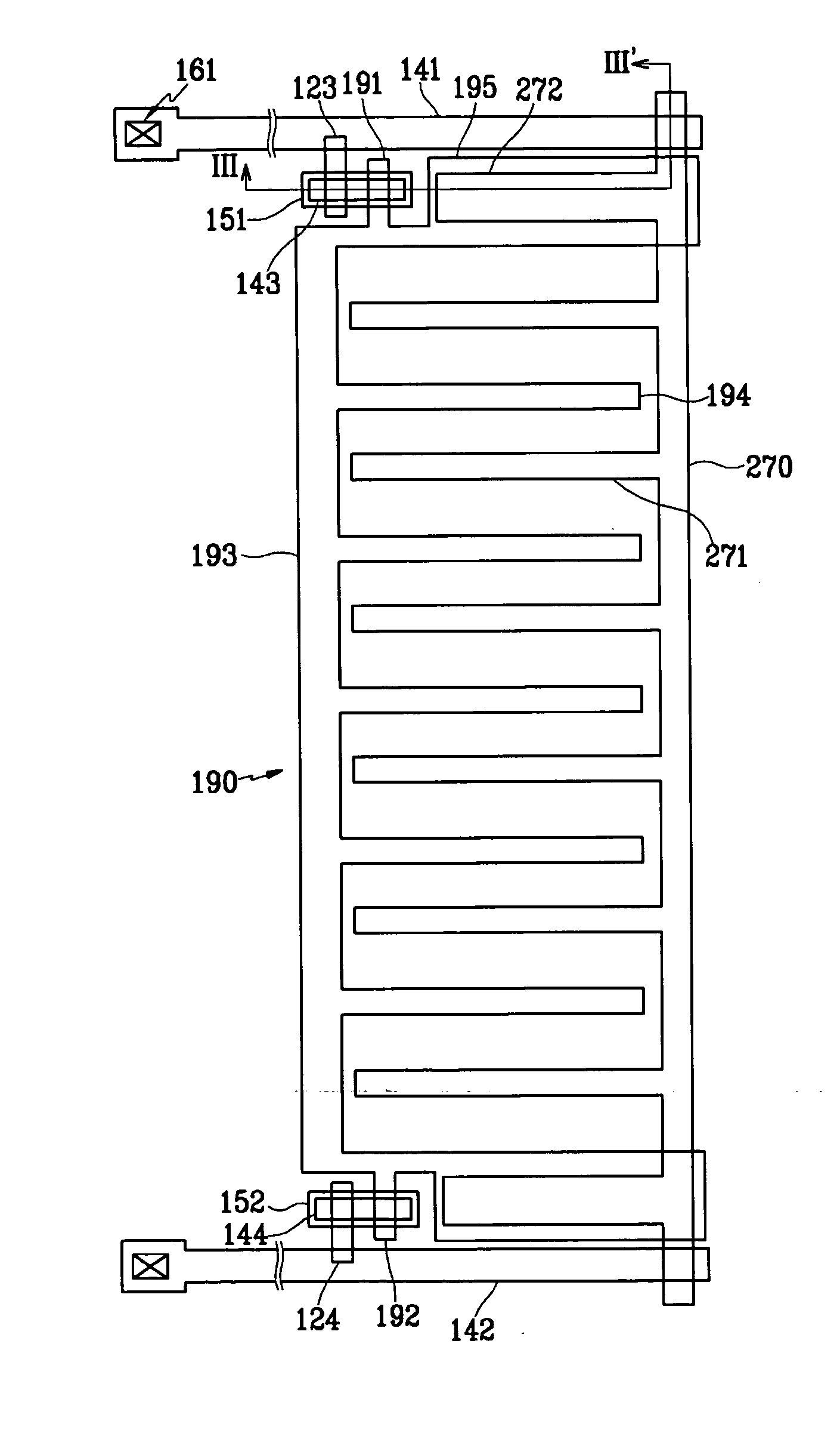
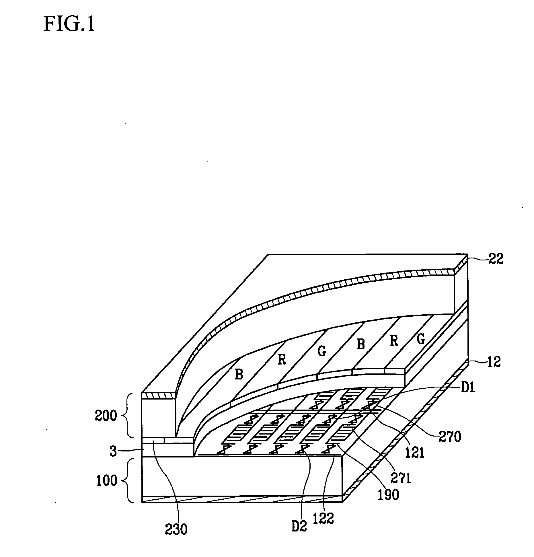
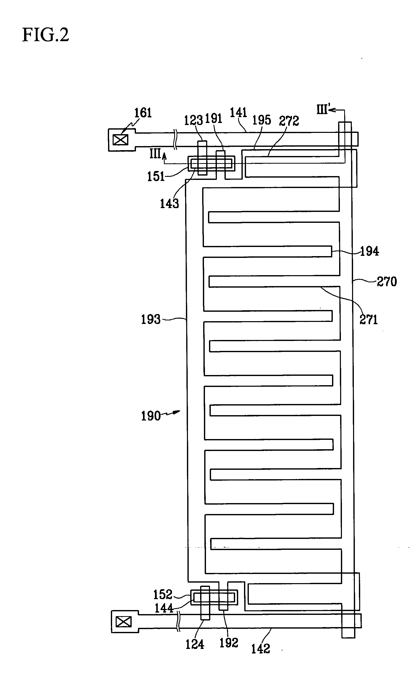
[0051] In the drawings, the thickness of layers, films, and regions are exaggerated for clarity. Like numerals refer to like elements throughout. It will be understood that when an element such as a layer, film, region, or substrate is referred to as being “on” another element, it can be directly on the other element or intervening elements may also be present. FIG. 1 is a perspective view of a liquid crystal display according to an embodiment of the present invention.

[0052...


PUM

PropertyMeasurementUnit
angleaaaaaaaaaa
angleaaaaaaaaaa
angleaaaaaaaaaa

Abstract

A thin film diode panel comprises a pixel electrode formed on a substrate, the pixel electrode including a stem portion and a plurality of branch portions extended from the stem portion, and a data electrode line formed on the substrate, the data electrode line including a plurality of branch electrodes formed parallel to the plurality of branch portions. The plurality of branch portions may extend in a direction perpendicular to the stem portion and the plurality of branch electrodes may extend in a direction perpendicular to the data electrode line.

Description

BACKGROUND OF THE INVENTION [0001] (a) Technical Field [0002] The present disclosure relates to thin film diode array panels using metal insulator metal (MIM) diodes as switching elements, and a manufacturing method of the same. In more detail, the present disclosure relates to thin film diode array panels of a dual select diode (DSD) type, and a liquid crystal display using the same. [0003] (b) Discussion of the Related Art [0004] A liquid crystal display (LCD) is one of the most widely used flat panel displays. An LCD includes two panels provided with field-generating electrodes, and a liquid crystal (LC) layer interposed therebetween. The LCD displays images by applying voltages to the field-generating electrodes to generate an electric field in the LC layer, which determines orientations of LC molecules in the LC layer to adjust polarization of incident light. [0005] An LCD may have switching elements to switch voltages of pixels arranged in a matrix form. An LCD can display var...

Claims


Application Information

Patent Timeline
Patent Type & Authority Applications(United States)
IPC IPC(8): G02F1/133G02F1/1337G02F1/1343G02F1/136G02F1/1362G02F1/1365H01L21/00H01L29/786H01L29/88H01L49/02
CPCG02F1/134363G02F2201/124G02F1/1365G02F1/13624
Inventor OH, JOON-HAKCHAI, CHONG-CHULSHIN, KYONG-JUKIM, JIN-HONGHONG, SUNG-JIN
Owner SAMSUNG DISPLAY CO LTD
Why Eureka
Try Eureka