Display control device

a display control and control device technology, applied in the direction of instruments, static indicating devices, etc., can solve the problems of increasing production costs and production costs, and achieve the effects of reducing the circuit layout area and the production cost of the display control device, suppressing the increase in production costs, and reducing the circuit layout area and production cos

Active Publication Date: 2007-07-05
RENESAS ELECTRONICS CORP
View PDF11 Cites 5 Cited by
  • Summary
  • Abstract
  • Description
  • Claims
  • Application Information

AI Technical Summary

Benefits of technology

[0022] In the display control device according to the present invention, as described above, the latch circuits are employed in the data hold block. As a result, a circuit layout area of the display control device can be reduced, and thereby the increase in its production cost can be suppressed. Even when the latch circuits are employed, the same function as of the D flip-flops can be achieved in the display control device. In other words, it is possible according to the present invention to reduce the circuit layout area and the production cost of the display control device with achieving the conventional function.

Problems solved by technology

Increase in the layout area of the display control device causes increase in its production cost.

Method used


Image

  • Display control device
  • Display control device
  • Display control device

Examples


first embodiment

1. First Embodiment

[0045] 1-1. Configuration

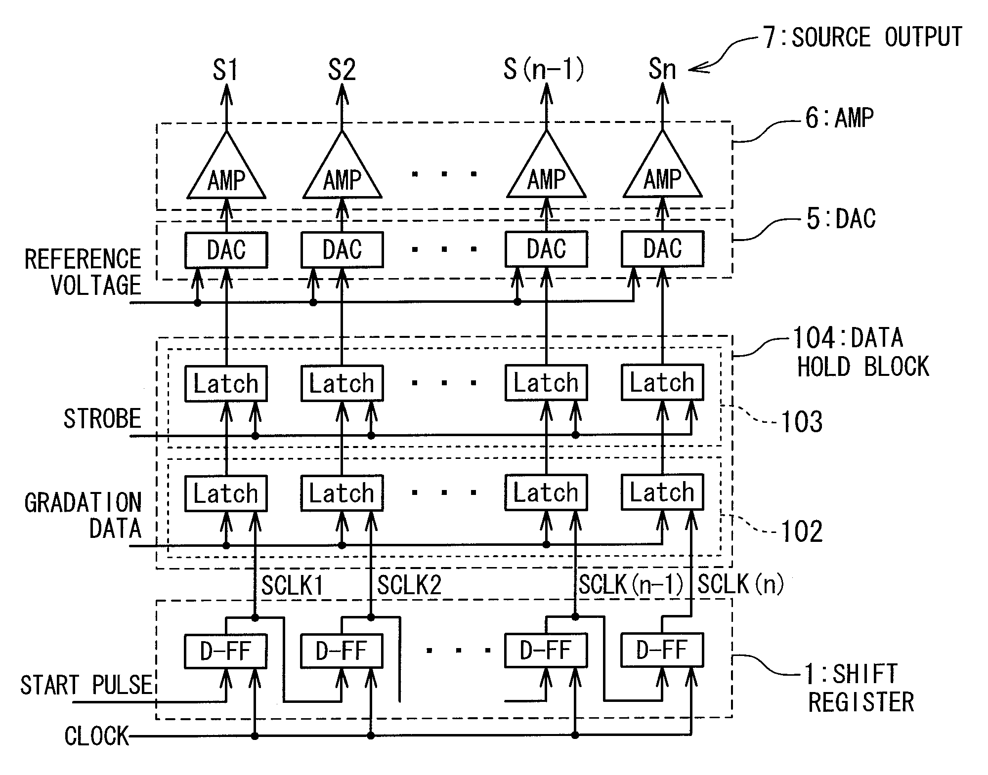
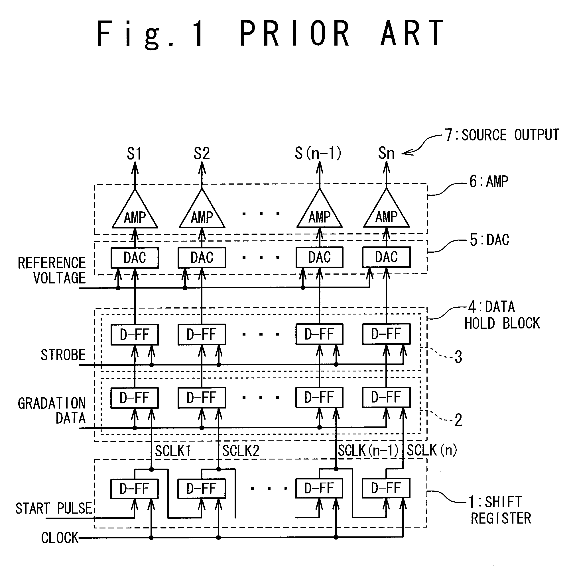
[0046]FIG. 7 is a block diagram showing a configuration of a display control device according to a first embodiment of the present invention. The display control device receives gradation data that are digital data corresponding to an image displayed on the display panel. Then, the display control device generates output voltages S1 to Sn (source output 7) corresponding to the received gradation data, and outputs the respective output voltages S1 to Sn to data lines of the display panel.

[0047] More specifically, the display control device is provided with a shift register 1, a data hold block 104, a DA converter 5 and an amplifier circuit 6, as shown in FIG. 7. The data hold block 104 is configured to hold the gradation data, and includes a data register 102 and a data latch 103. The shift register 1 is connected to the data register 102 of the data hold block 104. The data register 102 is connected to the data latch 103. The data latch ...

second embodiment

2. Second Embodiment

[0063] 2-1. Configuration

[0064]FIG. 11 is a block diagram showing a configuration of a display control device according to a second embodiment of the present invention. The same reference numerals are given to the same components as those described in the first embodiment, and an overlapping description will be appropriately omitted.

[0065] The display control device according to the present embodiment is provided with a data hold block 204 instead of the data hold block 104 shown in the first embodiment. The data hold block 204 includes the data register 102 and the data latch 103 as in the first embodiment. That is, the data register 102 has the n latch circuits associated with the n gradation data (n source outputs S1 to Sn) respectively. Moreover, the data latch 103 has the n latch circuits associated with the n gradation data (n source outputs S1 to Sn) respectively.

[0066] It should be noted that FIG. 11 illustrates in detail the inside of one latch circui...

third embodiment

3. Third Embodiment

[0079] 3-1. Configuration

[0080]FIG. 13 is a block diagram showing a configuration of a display control device according to a third embodiment of the present invention. The same reference numerals are given to the same components as those described in the foregoing embodiments, and an overlapping description will be appropriately omitted.

[0081] The display control device according to the present embodiment is provided with a data hold block 304 instead of the data hold block 104 shown in the first embodiment. The data hold block 304 has the same configuration as the data hold block 204 shown in the second embodiment. That is, the data hold block 304 includes the data register 102, the data latch 103, the OR circuits, the switch circuits 11 and 12. It should be noted that FIG. 13 illustrates in detail the inside of one latch circuit (one Latch shown in FIG. 7) for latching one gradation data associated with the output voltage S1. Hereinafter, let us consider a cas...


PUM


Abstract

A display control device has: a shift register generating n shift pulses in series; a data hold block configured to hold n gradation data; and a DA converter for converting the n gradation data into corresponding gradation voltages. The data hold block includes: n first latch circuits configured to respectively latch the n gradation data in series in synchronization with the n shift pulses; and n second latch circuits provided between the DA converter and the n first latch circuits. An electrical connection between the first latch circuits and the second latch circuits is cut off while the first latch circuits receive the n gradation data. After the first latch circuits finish latching all the gradation data, the n gradation data are simultaneously supplied to the DA converter from the first latch circuits through the second latch circuits.

Description

BACKGROUND OF THE INVENTION [0001] 1. Field of the Invention [0002] The present invention relates to a display control device for controlling a display. [0003] 2. Description of the Related Art [0004] A display such as an active-matrix liquid crystal display and the like is publicly known. A display control device is used for controlling image representation on the display. FIG. 1 is a block diagram schematically showing a configuration of a conventional display control device used in the liquid crystal display. FIG. 2 is a timing chart showing an operation of the display control device shown in FIG. 1. FIG. 3 is a circuit diagram showing a configuration of a typical D flip-flop. The conventional display control device will be described below with reference to FIGS. 1 to 3. [0005] As shown in FIG. 1, the display control device is provided with a shift register 1, a data hold block 4, a DA converter (DAC) 5 and an amplifier circuit (AMP) 6. The data hold block 4 includes a data regis...

Claims


Application Information

Patent Timeline
Patent Type & Authority Applications(United States)
IPC IPC(8): G09G3/36
CPCG09G3/3688G09G2310/027G09G2330/12G09G2310/08G09G2310/0294
Inventor ENDOU, SHINJIDOI, TAKAYUKI
Owner RENESAS ELECTRONICS CORP
Why Eureka
Try Eureka