Organic electroluminescence element

a technology of electroluminescence element and organic material, which is applied in the direction of organic semiconductor device, thermoelectric device, organic chemistry, etc., can solve the problems of inability to improve the efficiency of light emission cannot be reduced, so as to achieve small electricity consumption and high light emission efficiency

Inactive Publication Date: 2010-05-06
IDEMITSU KOSAN CO LTD
View PDF5 Cites 0 Cited by
  • Summary
  • Abstract
  • Description
  • Claims
  • Application Information

AI Technical Summary

Benefits of technology

[0006]The present invention has been made to overcome the above problem and has an object of providing an organic EL device exhibiting a high efficiency of light emission even at a high luminance of several thousand cd / m2 or greater and a small consumption of electricity.
[0029]It is preferable that the organometallic complex compound has the light emitting property to which the triplet state contributes and more preferably the light emitting property to which the triplet state contributes at the room temperature. In the light emission to which the triplet state contributes, the deactivation process of the excited state of the triplet is suppressed since the content of the polyacene-based condensed ring structure such as naphthalene and anthracene in the amine derivative is small. Therefore, the light emission to which the triplet state contributes can be efficiently performed and the device exhibiting a small consumption of electricity can be obtained.
[0032]It is preferable that the main material of the organic light emitting layer has an energy of the triplet level greater than an energy of the triplet level of the organometallic complex compound having a heavy metal. When this condition is satisfied, the energy of the main material of the organic light emitting layer is transferred efficiently to the organometallic complex compound and the efficiency of light emission is further increased.
[0038]It is preferable that at least one of the anode and the cathode is formed with a transparent or translucent material so that the light emitted from the organic light emitting layer is efficiently obtained at the outside.

Problems solved by technology

The device having the above construction has a drawback in that a marked decrease in the efficiency of light emission accompanies an improvement in the luminance of the emitted light and a problem arises in that the consumption of electricity of the flat panel display does not decrease due to this drawback.
However, the decrease in the efficiency of light emission cannot be improved as long as the hole transporting materials currently used for practical applications is used since the deactivation process of the triplet state is dominant in the high luminance region.

Method used


Image

  • Organic electroluminescence element
  • Organic electroluminescence element
  • Organic electroluminescence element

Examples


example 1

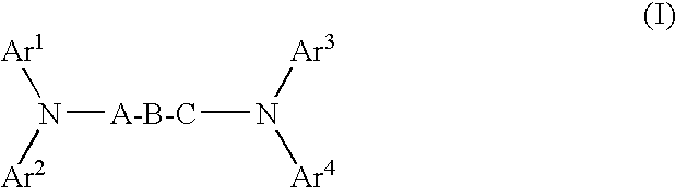
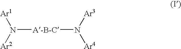
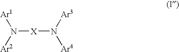
[0040]A glass substrate (manufactured by GEOMATEC Company) of 25 mm×75 mm×1.1 mm thickness having an ITO transparent electrode was cleaned by application of ultrasonic wave in isopropyl alcohol for 5 minutes and then by exposure to ozone generated by ultraviolet light for 30 minutes. The glass substrate having the transparent electrode lines which had been cleaned was attached to a substrate holder of a vacuum vapor deposition apparatus and cleaned with plasma under the atmosphere of a mixture of oxygen and argon. On the surface of the cleaned substrate at the side having the transparent electrode lines, a film of compound 1 shown below, which was a compound represented by general formula (I′), having a thickness of 50 nm was formed in a manner such that the formed film covered the transparent electrode. The formed film of compound 1 worked as the hole transporting layer. On the formed film, 4,4′-N,N′-dicarbazolebiphenyl (CBP) and tris(2-phenylpyridyl)iridium (Ir(Ppy)) were binary v...

example 2

[0042]An organic EL device was prepared in accordance with the same procedures as those conducted in Example 1 except that compound 2 shown in the following which was a compound represented by general formula (I) was used in place of compound 1.

[0043]The luminance of the obtained organic EL device was measured under various voltages and electric currents and the efficiency of light emission (=(luminance) / (current density)) at the luminance of emitted light of 10,000 cd / m2 was calculated. The efficiency of light emission was found to be 37 cd / A.

example 3

[0044]An organic EL device was prepared in accordance with the same procedures as those conducted in Example 1 except that compound 3 shown in the following which was a compound represented by general formula (I) was used in place of compound 1.

[0045]The luminance of the obtained organic EL device was measured under various voltages and electric currents and the efficiency of light emission (=(luminance) / (current density)) at the luminance of emitted light of 10,000 cd / m2 was calculated. The efficiency of light emission was found to be 50 cd / A.


PUM

PropertyMeasurementUnit
luminanceaaaaaaaaaa
luminanceaaaaaaaaaa
work functionaaaaaaaaaa

Abstract

In an organic electroluminescence device having a pair of electrodes and an organic medium which has a light emitting layer or a plurality of layers including the light emitting layer, contains a light emitting material formed with an organometallic complex compound having a heavy metal and is disposed between the pair of electrodes, the organic medium contains an amine derivative having a specific structure. The organic electroluminescence device exhibits a high efficiency of light emission even at a high luminance of several thousand cd / m2 or greater and a small consumption of electricity.

Description

[0001]This application is a continuation of U.S. patent application Ser. No. 11 / 362,209, filed on Feb. 27, 2006, Ser. No. 10 / 477,752, filed on Nov. 24, 2003, and claims priority to U.S. patent application Ser. No. 10 / 477,752, filed on Nov. 24, 2003, International Patent Application No. PCT / JP02 / 04485, filed on May 8, 2002, and Japanese Patent Application No. 2001-155290, filed on May 24, 2001, all of which are incorporated herein by reference in their entireties.TECHNICAL FIELD[0002]The present invention relates to an organic electroluminescence device used as a planar light emitting member of wall televisions and a light source for a back light of displays, and more particularly, to an organic electroluminescence device exhibiting a high efficiency of light emission even at a high luminance and a small consumption of electricity.BACKGROUND ART[0003]Organic electroluminescence (“electroluminescence” will be referred to as “EL”) devices which utilize organic substances are expected t...

Claims


Application Information

Patent Timeline
Patent Type & Authority Applications(United States)
IPC IPC(8): H01L51/50H01L33/00C09K11/06H01L51/00H01L51/30
CPCC09K11/06C09K2211/1003C09K2211/1007C09K2211/1011C09K2211/1014H01L51/0059H01L51/006H01L51/0081H01L51/0084H01L51/0085H01L51/0086H01L51/50H01L51/5012H01L2251/308H10K85/633H10K85/631H10K85/341H10K85/344H10K85/324H10K85/342H10K50/11H10K2102/103C07D213/16C09K2211/185H10K50/00
Inventor MATSUURA, MASAHIDEHOSOKAWA, CHISHIO
Owner IDEMITSU KOSAN CO LTD
Why Eureka
Try Eureka