

Charge transporting material, organic electroluminescent element, and light emitting panel
a technology of organic electroluminescent elements and charge transporting materials, applied in the direction of discharge tubes/lamp details, discharge tubes luminescnet screens, natural mineral layered products, etc., can solve the problems of large amount (about 5 to 10 percent) of doping, and the difficulty of producing a large substrate. , to achieve the effect of excellent charge transporting ability and highly adaptable to electronic devices
- Summary
- Abstract
- Description
- Claims
- Application Information
AI Technical Summary
Benefits of technology
Problems solved by technology
Method used
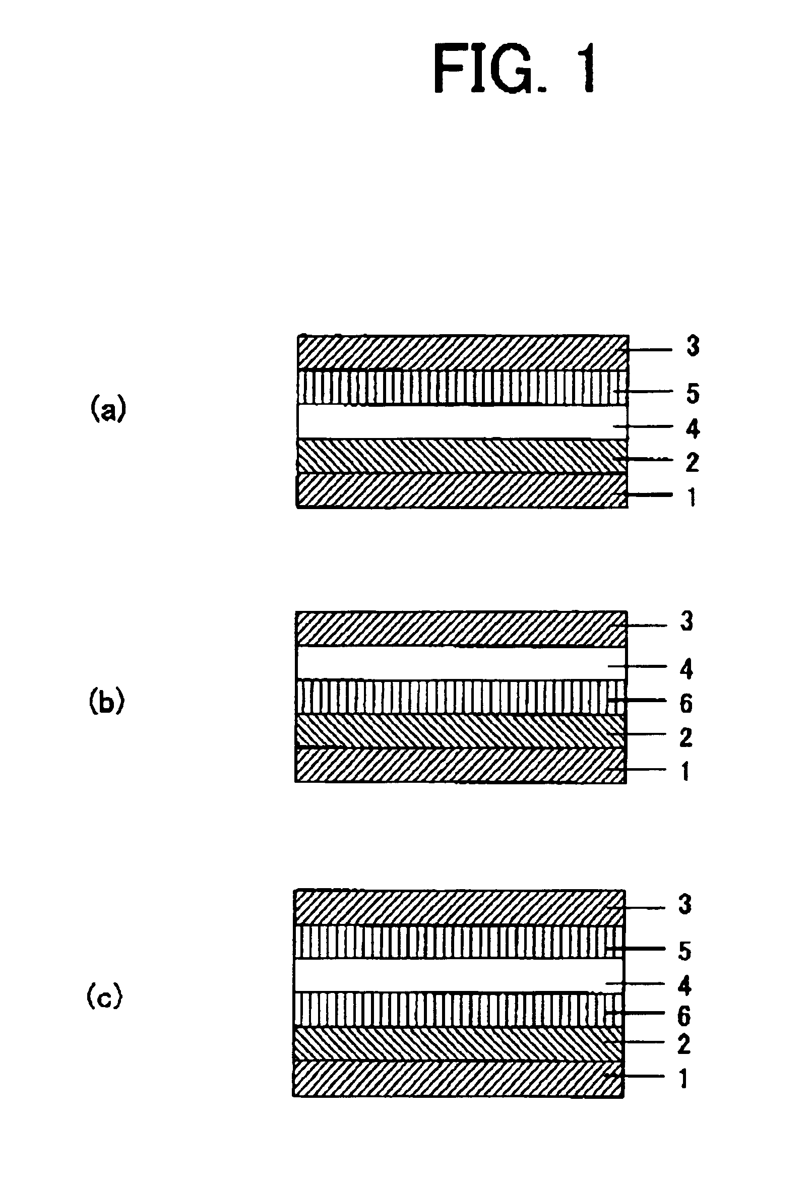
Image

Examples
examples
[0108]Though the present invention will be hereinafter explained by way of examples, the scope of the present invention is not restricted by these examples.
examples a series
Example A1
[0109]0.80 g of phosphorus oxychloride was added into 50 mL of N,N-dimethylformamide and stirred at room temperature to be dissolved. Herein, a solution prepared by dissolving 2.42 g of CBP in 15 mL of dry chloroform was added and stirred at room temperature to obtain formyl-product of CBP (4-(Carbazol-9-yl)-4′-(3-formylcarbazol-9-yl)-biphenyl). On the other hand, 1.83 g of triphenylphosphine was added into 50 mL of benzene to be dissolved. Then 0.67 g of bromomethane was added therein and stirred at room temperature to produce phosphonium salt. The phosphonium salt thus obtained was dissolved in 50 mL of dry diethyl ether under dry nitrogen flow, and 4.4 mL of butyl lithium solution in hexane (1.6 M) was further added and stirred at room temperature to produce phosphoylide. Then 2.18 g of the formyl-product of CBP which is dissolved in 20 mL of dry diethyl ether was further added therein to allow Wittig reaction, thereby producing vinyl-product of CBP (4-(Carbazol-9-yl)-4...
examples b series
Production Example B1
[0116]0.80 g of phosphorus oxychloride was added into 50 mL of N,N-dimethyl formamide and stirred at room temperature to be dissolved. Herein, a solution prepared by dissolving 2.42 g of CBP in 15 mL of dry chloroform was added and stirred at room temperature to obtain formyl-product of CBP (4-(Carbazol-9-yl)-4′-(3-formylcarbazol-9-yl)-biphenyl). On the other hand, 1.83 g of triphenylphosphine was added into 50 mL of benzene to be dissolved. Then 0.67 g of bromomethane was added therein and stirred at room temperature to produce phosphonium salt. The phosphonium salt thus obtained was dissolved in 50 mL of dry diethyl ether under dry nitrogen flow, and 4.4 mL of butyl lithium solution in hexane (1.6 M) was further added and stirred at room temperature to produce phosphoylide. Then 2.18 g of the formyl-product of CBP which is dissolved in 20 mL of dry diethyl ether was further added therein to allow Wittig reaction, thereby producing vinyl-product of CBP (4-(Carb...
PUM
| Property | Measurement | Unit |
|---|---|---|
| thickness | aaaaa | aaaaa |
| inner quantum efficiency | aaaaa | aaaaa |
| inner quantum efficiency | aaaaa | aaaaa |
Abstract
Description
Claims
Application Information