Organic material and photoelectric conversion element

a photoelectric conversion element and organic material technology, applied in the direction of non-metal conductors, conductors, organic chemistry, etc., can solve the problems of difficult to obtain high open circuit voltage, high cost of silicon solar cells typified by silicon solar cells, and inferior diffusion length of separated electric charges

Active Publication Date: 2015-10-01
RICOH KK +1
View PDF11 Cites 8 Cited by
  • Summary
  • Abstract
  • Description
  • Claims
  • Application Information

AI Technical Summary

Benefits of technology

[0015]The present invention can provide a novel organic material which has a high open circuit voltage, can absorb light of a wide wavelength range, and is excellent in charge transport ability when it is applied to an organic thin film solar cell system. The novel organic material can solve the existing problems.

Problems solved by technology

However, existing solar cells typified by silicon solar cells are costly at present, which is a factor of preventing them from being widely used.
However, organic materials have an exciton diffusion length of about only several nanometers, and a diffusion length of the separated electric charge is also much inferior to silicon or the like although it cannot flatly be said since the diffusion length is greatly influenced by its crystalline state.
However, the conjugated polymers have a problem in that it is difficult to obtain high open circuit voltage since their ionization potential, which is a material property correlated to the open end voltage, is low due to extended conjugation thereof.
Moreover, they are polymers and have a molecular weight distribution, which causes a problem in that stable materials are difficult to obtain during production.
However, the former has a high ionization potential and a high open circuit voltage, but it can absorb light of short wavelengths, and thus is insufficient in photoelectric conversion efficiency.
Meanwhile, the latter can absorb light of relatively longer wavelengths, but it is poor in aggregated structure responsible for charge transport path and charge separation, and thus is still insufficient in photoelectric conversion efficiency.

Method used


Image

  • Organic material and photoelectric conversion element
  • Organic material and photoelectric conversion element
  • Organic material and photoelectric conversion element

Examples


synthesis example 1

[0089]In accordance with the following scheme, 2DPP-TBDT, which is the Exemplary Compound 2, was synthesized. Note that, compound 7 described in the scheme was synthesized based on Angewandte Chemie, International Edition (2011), 50, (41), 9697-9702.

[0090]Compound 1 (10.0 g, 33.3 mmol), 2-ethylhexyl bromide (19.3 g, 99.9 mmol), and K2CO3 (18.4 g, 133 mmol) were mixed in a dry DMF (300 mL), and were stirred at 120° C. for 24 hours. After cooling to room temperature, the reaction mixture was poured into a large amount of ice water in order to form precipitates. The obtained precipitates were collected through a filtration, and were washed with water and methanol.

[0091]The obtained product was purified by silica gel column chromatography (eluent: CHCl3 / hexane=1:1, v / v), was recrystallized with CHCl3 / methanol, and was dried under vacuum, to thereby obtain compound 2 as a reddish brown solid (8.89 g, yield=51%).

[0092]The results of 1H NMR and 13C NMR for the obtained compound 2 are shown...

example 1

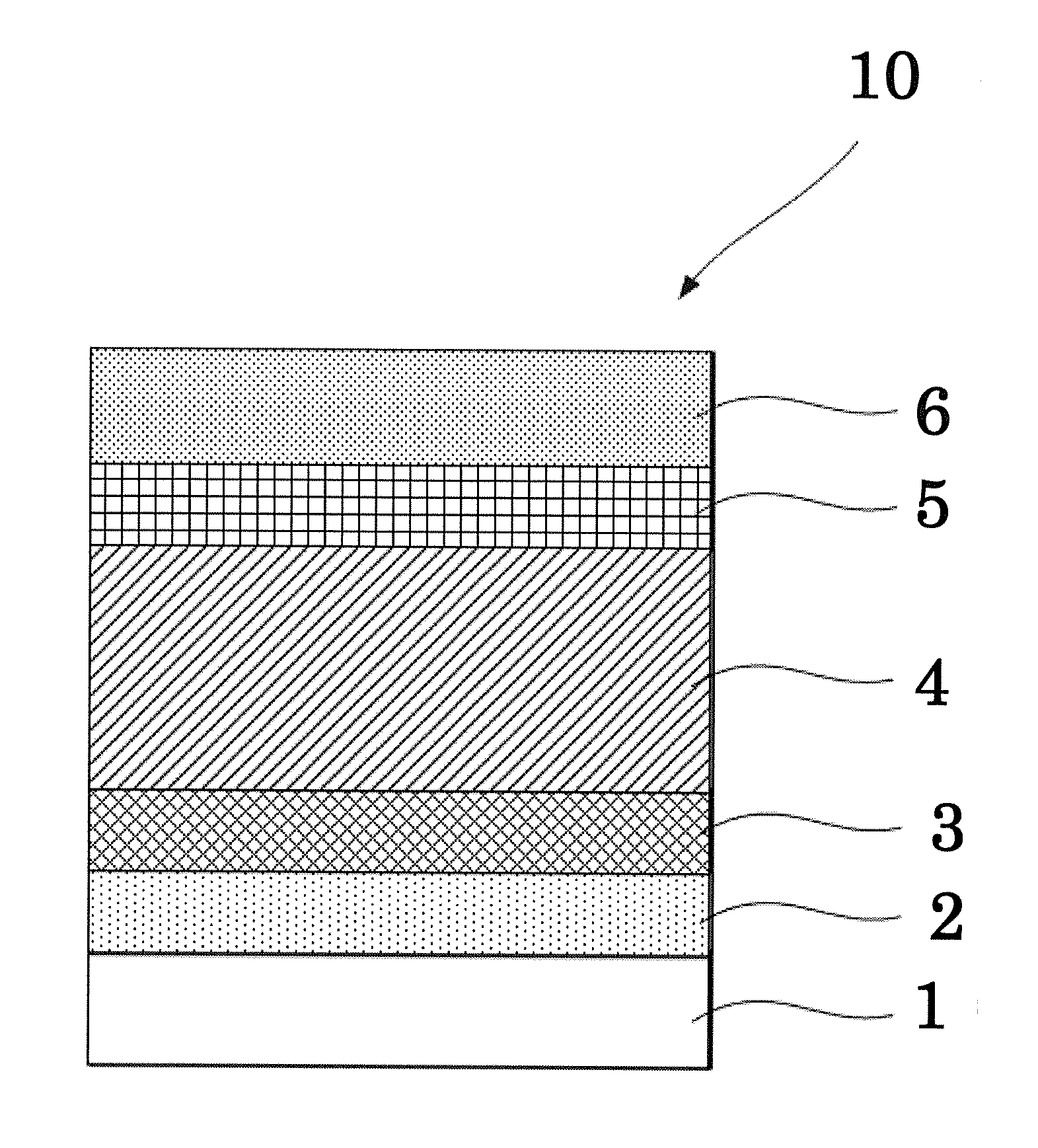
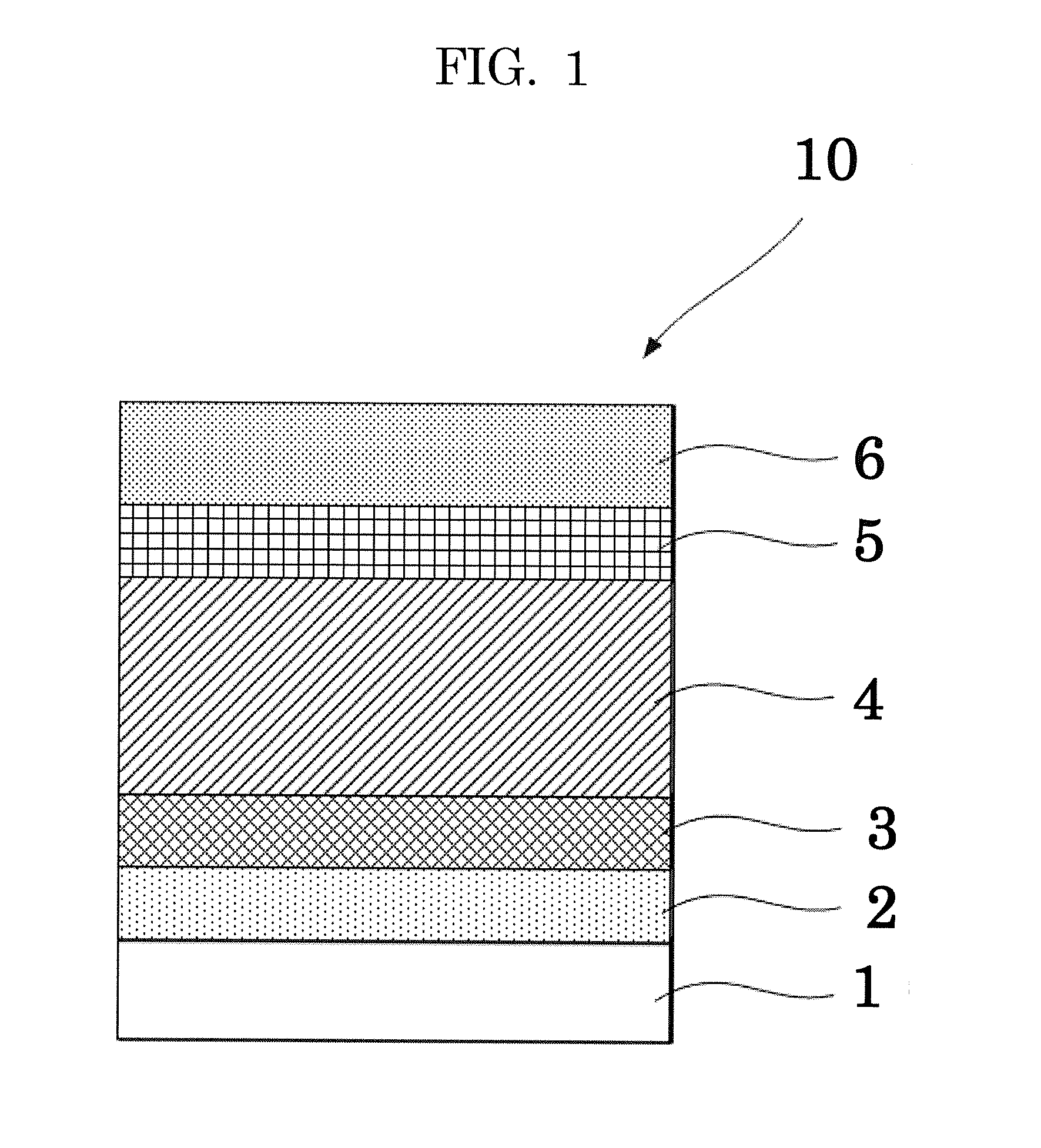
[0134]A solution of PEDOT:PSS was coated on a glass substrate with a patterned ITO that had been subjected to ultrasonic washing and UV ozone cleaning in the same manner as in Comparative Example 1.

[0135]Next, an organic material shown in the Exemplary Compound 2 and PC71BM (phenyl C71 butyric acid methyl ester, product of Frontier Carbon Corporation) were dissolved in chloroform (1 mL) at a ratio of 7 mg:7 mg. The resultant mixture was stirred overnight or longer in a glove box that had been purged with nitrogen, to thereby prepare a solution for forming a photoelectric conversion layer.

[0136]Then, the obtained solution for forming a photoelectric conversion layer was coated on the PEDOT:PSS film in the atmosphere by a spin coating method, to thereby form a film thereon. Then, the film was dried at 120° C. for 10 minutes, to thereby form a photoelectric conversion layer. The obtained photoelectric conversion layer was found to have an average thickness of 110 nm.

[0137]Next, using a...

example 2

Preparation of Photoelectric Conversion Element

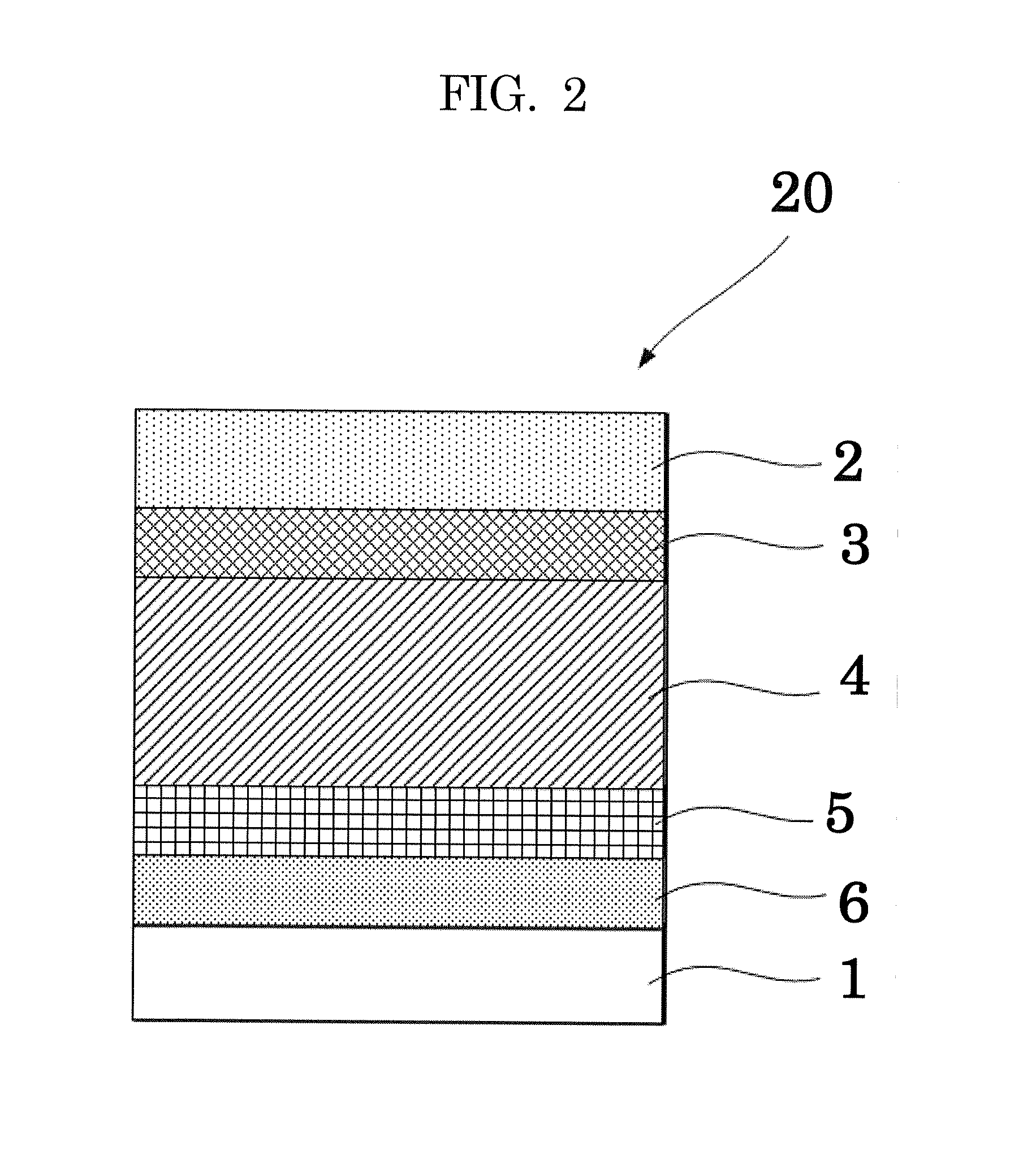
[0139]A photoelectric conversion element was prepared in the same manner as in Example 1 except that diiodooctane was added to the solution for forming a photoelectric conversion layer so that a concentration thereof was 1% by mass.

[0140]Note that, an addition of a small amount of diiodooctane to the solution for forming a photoelectric conversion layer prevents an excessive aggregation, and can form an appropriate aggregated structure for charge separation and charge transportation.

[0141]Solar cell performances of the prepared photoelectric conversion element were measured upon irradiation of simulated solar light (AM1.5, 100 mW / cm2) in the same manner as in Comparative Example 1. The obtained photoelectric conversion element was found to have an open end voltage of 720 mV, a short-circuit current density of 13.99 mA / cm2, a fill factor of 0.53, and a photoelectric conversion efficiency of 5.38%, which showed good photoelectric conversi...


PUM

PropertyMeasurementUnit
concentrationaaaaaaaaaa
temperatureaaaaaaaaaa

Abstract

An organic material represented by the following General Formula (1):where in the General Formula (1), R1 and R2, which may be identical to or different from each other, each represent an alkyl group having 4 to 24 carbon atoms, X represents a substituted or unsubstituted aromatic hydrocarbon group, Y represents an aromatic hydrocarbon group, an alkoxyl group, or an alkyl group, which may be substituted with a substituent, and n represents an integer of 1 to 3.

Description

BACKGROUND OF THE INVENTION[0001]1. Field of the Invention[0002]The present invention relates to organic materials and a photoelectric conversion element using the same.[0003]2. Description of the Related Art[0004]In recent years, importance of solar cells has been increasing as an alternative energy to fossil fuel and as a measure against global warming. However, existing solar cells typified by silicon solar cells are costly at present, which is a factor of preventing them from being widely used. Therefore, research and development on various low-cost solar cells have been advancing. In particular, one example thereof is an organic thin film solar cell. The organic thin film solar cell is lightweight, low-priced, and easily enlarged in its surface area. Thus, expectations for practical applications have been increased. However, the photoelectric conversion efficiency of the organic thin film solar cell is still ½ or less that of the silicone-based solar cells.[0005]A photoelectric...

Claims


Application Information

Patent Timeline
Patent Type & Authority Applications(United States)
IPC IPC(8): H01L51/00H01L51/44C07D495/04
CPCH01L51/0074C07D495/04H01L51/0072H01L51/442H01L51/0046H01L51/0037H01L51/0068Y02E10/549H10K85/655H10K85/6576H10K30/30H10K85/6572H10K30/82H10K85/211H10K85/1135
Inventor ARAI, RYOTAHIDAKA, YUSHIN, WOONGADACHI, CHIHAYAYASUDA, TAKUMA
Owner RICOH KK
Why Eureka
Try Eureka