Eureka AIR delivers breakthrough ideas for toughest innovation challenges, trusted by R&D personnel around the world.

Alkali metal doping method in large-scale production of CIGS (copper, indium, gallium, selenium) thin-film solar cell

A technology for solar cells and copper indium gallium selenide, which is applied in the field of solar cells, can solve problems such as the inability to effectively improve the photoelectric conversion efficiency of copper indium gallium selenide cells, and achieves low device and production process costs, improved filling factor, and simple operation. Effect

Active Publication Date: 2013-12-25
ZHEJIANG SHANGYUE OPTOELECTRONICS TECH
View PDF8 Cites 27 Cited by
  • Summary
  • Abstract
  • Description
  • Claims
  • Application Information

AI Technical Summary

Problems solved by technology

However, due to the different solid solubility of sodium to copper, indium, and gallium materials, this method will limit the lattice growth of copper indium selenide while promoting the lattice growth of copper indium selenide, and cannot effectively improve the copper indium selenium lattice growth. Photoelectric Conversion Efficiency of Gallium Selenium Cells

Method used


Image

  • Alkali metal doping method in large-scale production of CIGS (copper, indium, gallium, selenium) thin-film solar cell
  • Alkali metal doping method in large-scale production of CIGS (copper, indium, gallium, selenium) thin-film solar cell
  • Alkali metal doping method in large-scale production of CIGS (copper, indium, gallium, selenium) thin-film solar cell

Examples


Embodiment Construction

[0038] In order to make the technical problems, technical solutions and beneficial effects solved by the present invention clearer, the present invention will be further described in detail below in conjunction with the accompanying drawings and embodiments. It should be understood that the specific embodiments described here are only used to explain the present invention, not to limit the present invention.

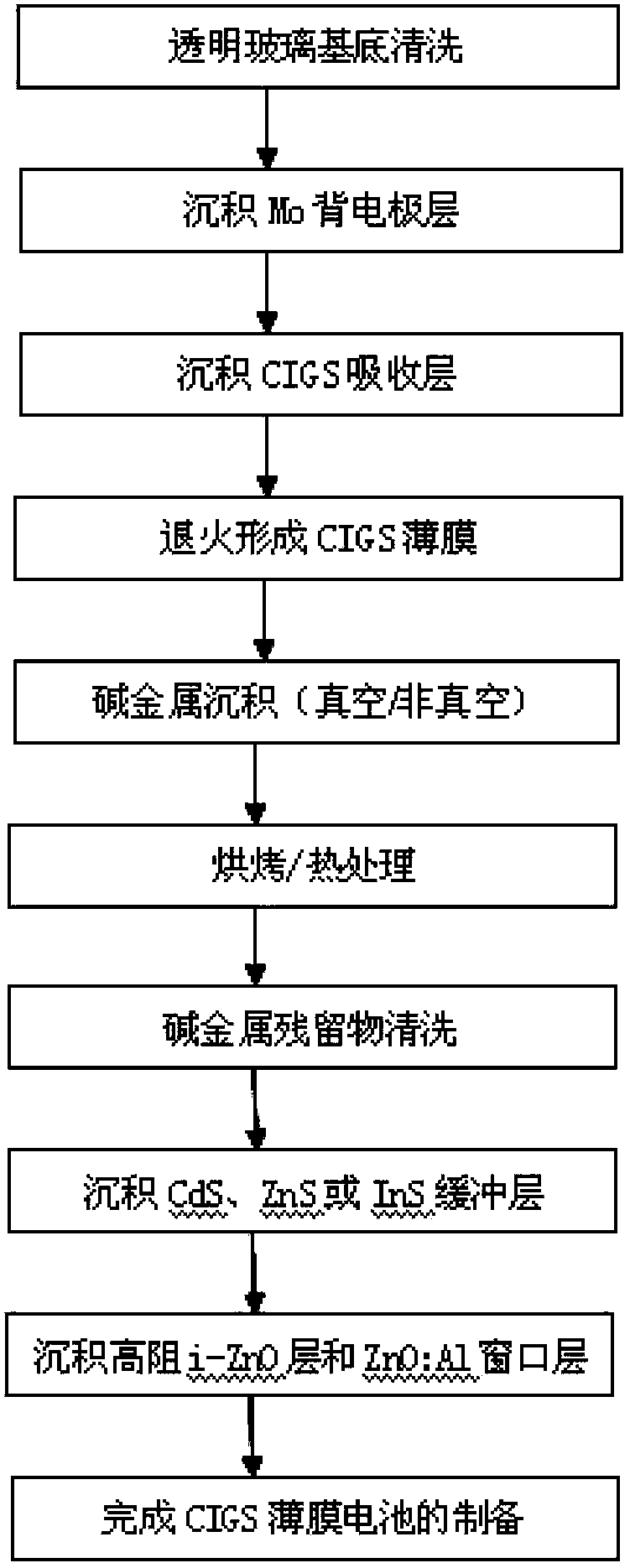
[0039] Such as figure 1 Shown, illustrate the flowchart of the alkali metal doping method in a kind of thin film material according to an embodiment of the present invention, comprise following process:

[0040]1. Cleaning is used to provide transparent glass as a substrate;

[0041] 2. Utilize the sputtering process to cover the back electrode Mo layer on the above-mentioned transparent glass substrate;

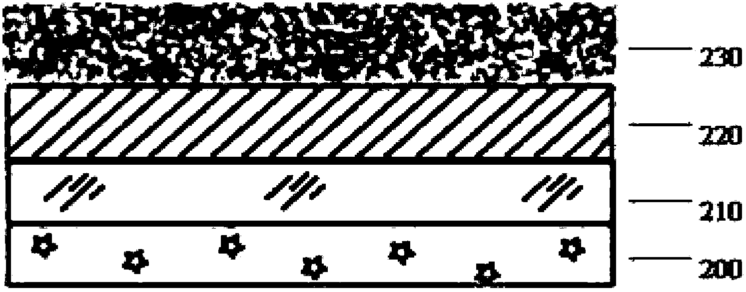
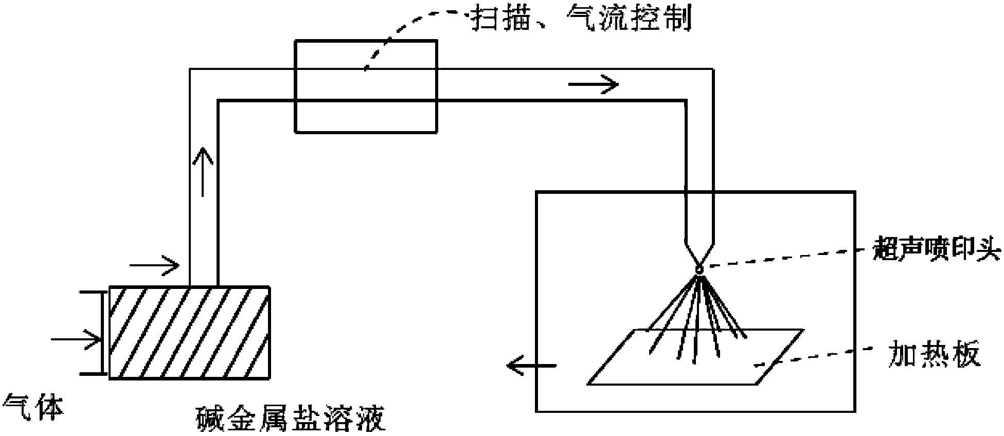
[0042] 3. Use the spraying process to spray the CIGS precursor on the basis of the previous steps, thereby depositing and forming a light-absorbing layer including c...


PUM


Abstract

Provided is an alkali metal doping method in the large-scale production of CIGS (copper, indium, gallium, selenium) thin-film solar cells. The method comprises a step of depositing an Mo metal back electrode layer on a glass substrate, a stainless indium substrate or a flexible substrate; a step of preparing a CIGS optical absorption layer; performing alkali metal element doping and deposition on the CIGS optical absorption layer; a step of performing thermal treatment on the alkali metal thin film formed after the deposition so as to make the alkali metal permeate into a CIGS crystal boundary and to improve characteristics of the crystal boundary; a step of cleaning alkali metal residues; a step of depositing a CdS, ZnS or InS buffer layer on the CIGS thin film after the cleaning of the alkali metal residues; and a step of depositing a high-resistance i-ZnO layer and a high-resistance ZnO:Al window layer, and thus a CIGS solar cell is formed. According to the alkali metal doping method, after annealing, the permeation of the alkali metal does not affect the generation of the CIGS crystal lattices; after the permeation of the alkali metal into the CIGS optical absorption layer, filling factors are substantially improved and the cell photoelectric conversion efficiency is improved when the open circuit voltage is improved.

Description

technical field [0001] The invention relates to the technical field of solar cells, in particular to an alkali metal doping method in large-scale production of copper indium gallium selenium thin film solar cells. Background technique [0002] Copper indium gallium selenide solar cells, that is, CIGS thin film solar cells, are chalcopyrite crystalline thin film solar cells with the best ratio of four elements: Cu (copper), In (indium), Ga (gallium), and Se (selenium). The key technologies that make up the solar panel. Because this product has many advantages such as strong light absorption capacity, good power generation stability, high conversion efficiency, long daytime power generation time, high power generation, low production cost and short energy recovery cycle, CIGS solar cells are already the future of solar cell products. star, can compete with traditional crystalline silicon solar cells. [0003] Alkali metal doping of the CIGS absorbing layer: refers to doping ...

Claims


Application Information

Patent Timeline
Patent Type & Authority Applications(China)
IPC IPC(8): H01L31/18
CPCY02P70/50
Inventor 任宇航任宇珂
Owner ZHEJIANG SHANGYUE OPTOELECTRONICS TECH
Why Eureka
Eureka Blog
Learn More