
Nonvolatile memory device and method of operating the same
a memory device and non-volatile technology, applied in the field of non-volatile memory devices and methods of operating the same, can solve the problems of increasing the consumption of current, increasing the operation time, the operating current, and the physical properties of the memory cells, so as to reduce the operation time or the operating current, and increase the efficiency of the operation of the memory device.
- Summary
- Abstract
- Description
- Claims
- Application Information
AI Technical Summary
Benefits of technology
Problems solved by technology
Method used
Image


Examples
Embodiment Construction
[0018]Hereinafter, some exemplary embodiments of the present disclosure will be described in detail with reference to the accompanying drawings. The figures are provided to enable those of ordinary skill in the art to make and use the embodiments of the disclosure.
[0019]Nonvolatile Memory Device
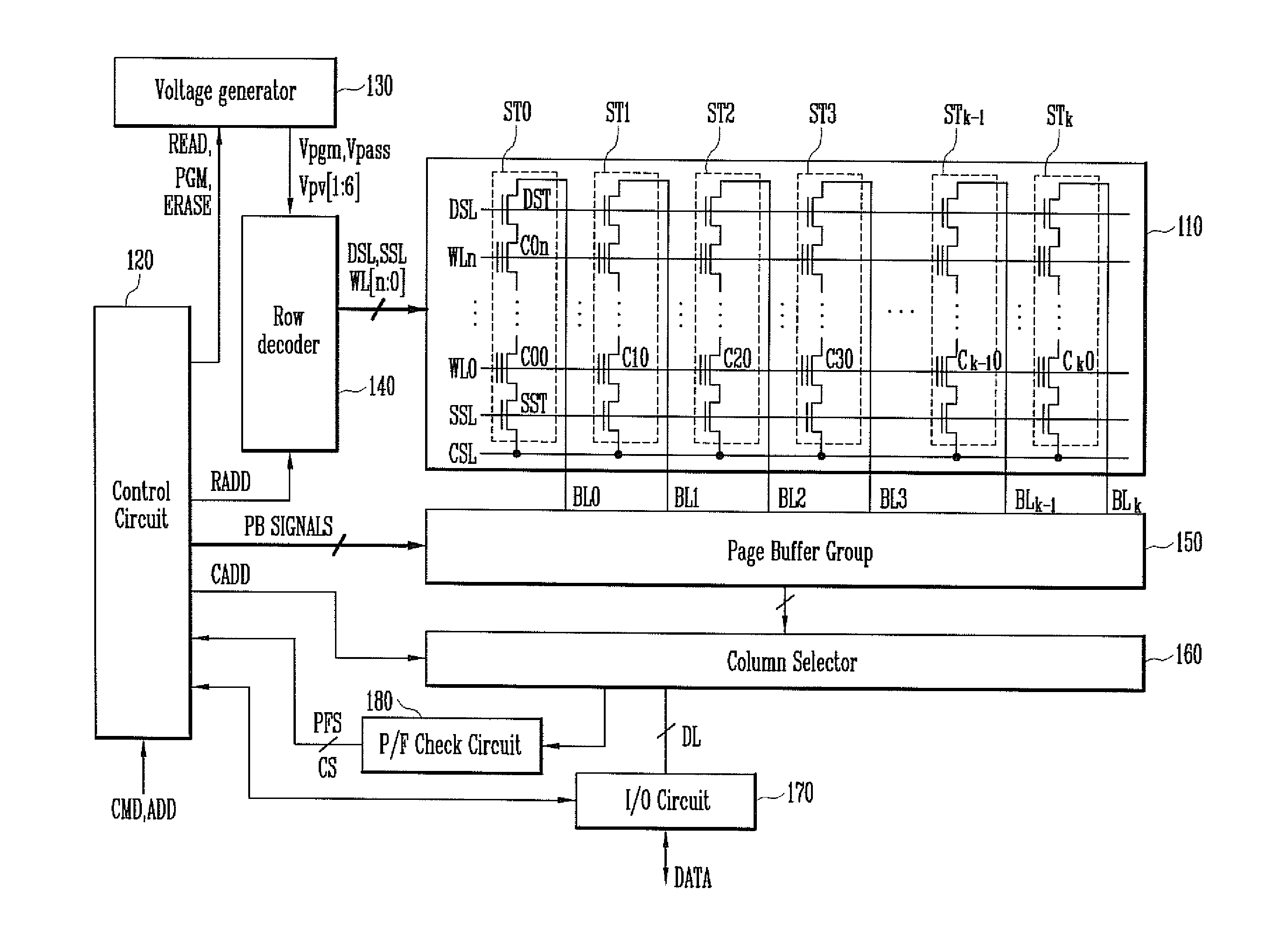
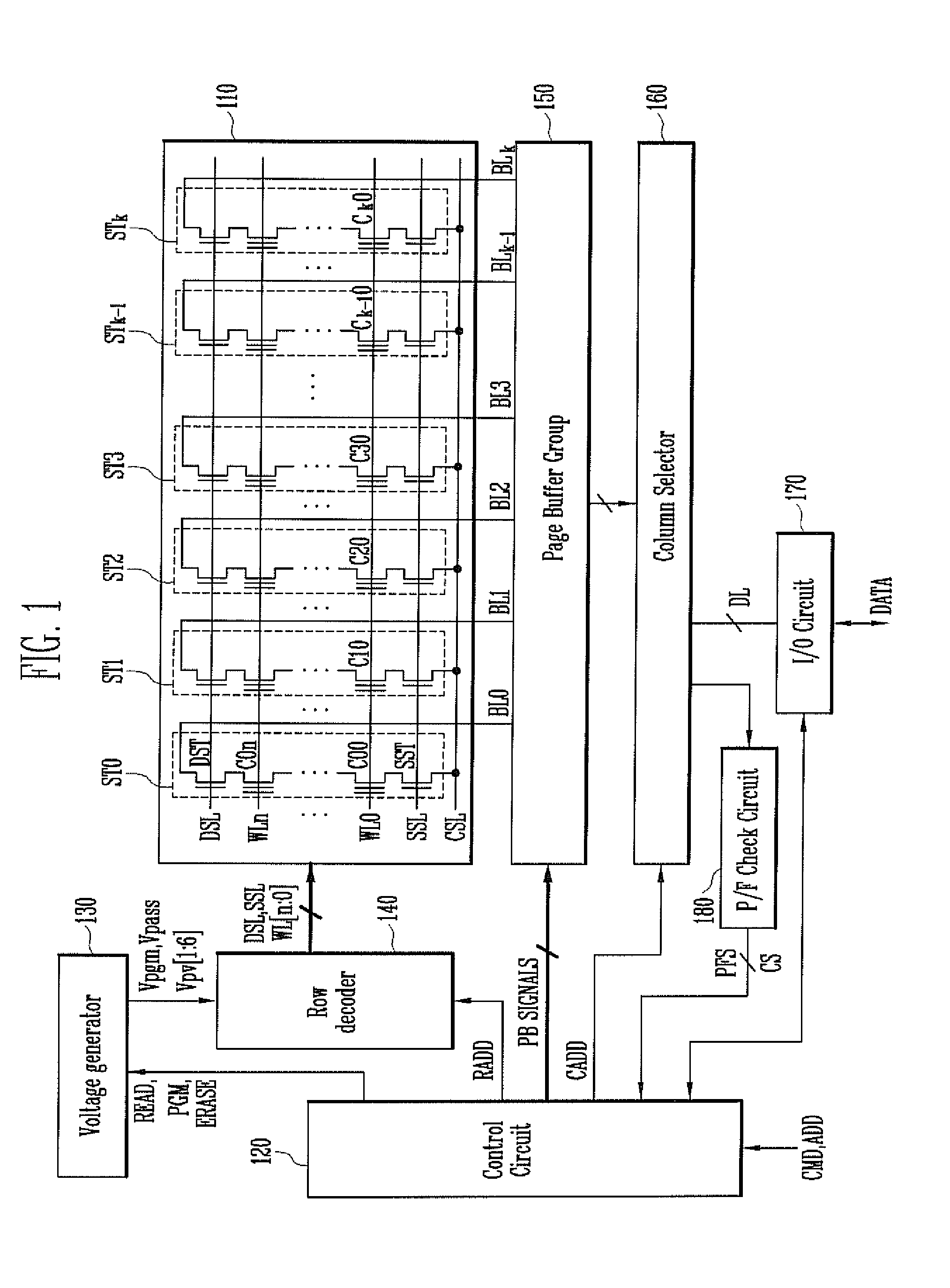
[0020]FIG. 1 is a block diagram showing a nonvolatile memory device according to an exemplary embodiment of this disclosure.
[0021]Referring to FIG. 1, the nonvolatile memory device according to the exemplary embodiment of this disclosure includes a memory cell block 110 included in a memory cell array, an operation circuit group (130, 140, 150, 160, 170, and 180) configured to perform a program operation, a program verification operation, an erase operation, and an erase verification operation for the memory cells of the memory cell block 110, and a control circuit 120 configured to control the operation circuit group (130, 140, 150, 160, 170, and 180).
[0022]In a NAND flash memory device, the...
PUM
 Abstract
Description
Claims
Application Information