Semiconductor structure and method of manufacturing the same

Active Publication Date: 2014-09-18
MACRONIX INT CO LTD
View PDF2 Cites 7 Cited by
  • Summary
  • Abstract
  • Description
  • Claims
  • Application Information

AI Technical Summary

Benefits of technology

[0006]The objective of the present invention is to provide a suitable semiconductor structure for a specific high voltage application, in which said semiconductor structure properly shunts the high voltage surge before said high stress damages the high voltage resistor in the conventional structure, and allows the semiconductor structure to withstand a higher breakdown voltage. A guard path including a capacitor and a diode having a high breakdown voltage is devised in said struc

Problems solved by technology

In the case of when a high voltage surge occurs to the I/O pad of the HVIC, the poly-silicon resistor itself can be dam

Method used


Image

  • Semiconductor structure and method of manufacturing the same
  • Semiconductor structure and method of manufacturing the same
  • Semiconductor structure and method of manufacturing the same

Examples


Embodiment Construction

[0019]The embodiments of the present invention are described more fully hereinafter with reference to the accompanying drawings, which form a part hereof, and which show, by way of illustration, specific exemplary embodiments by which the invention may be practiced. This invention may, however, be embodied in many different forms and should not be construed as limited to the embodiments set forth herein; rather, these embodiments are provided so that this disclosure will be thorough and complete, and will fully convey the scope of the invention to those skilled in the art. As used herein, the term “or” is an inclusive “or” operator, and is equivalent to the term “and / or,” unless the context clearly dictates otherwise. In addition, throughout the specification, the meaning of “a,”“an,” and “the” include plural references.

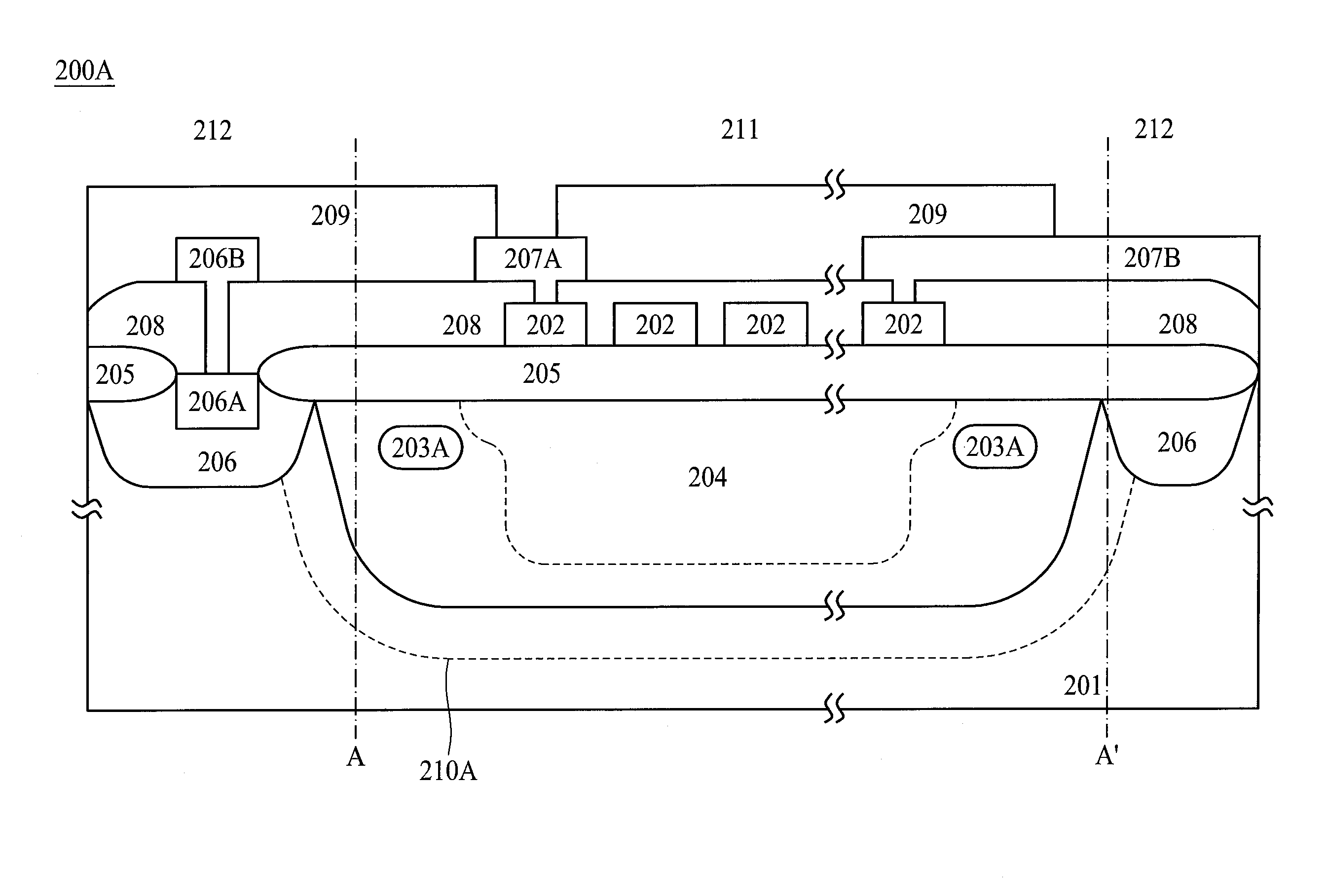
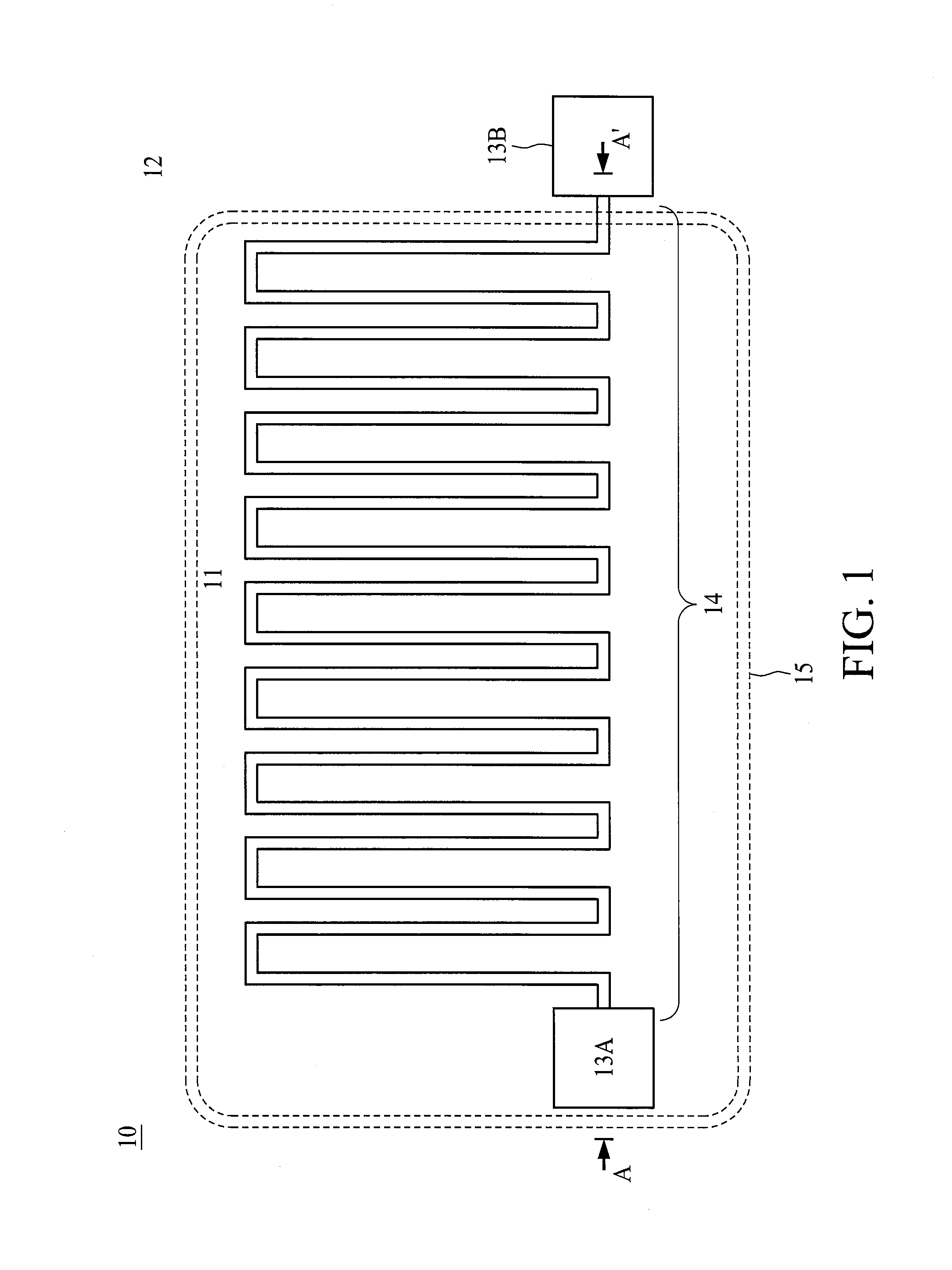
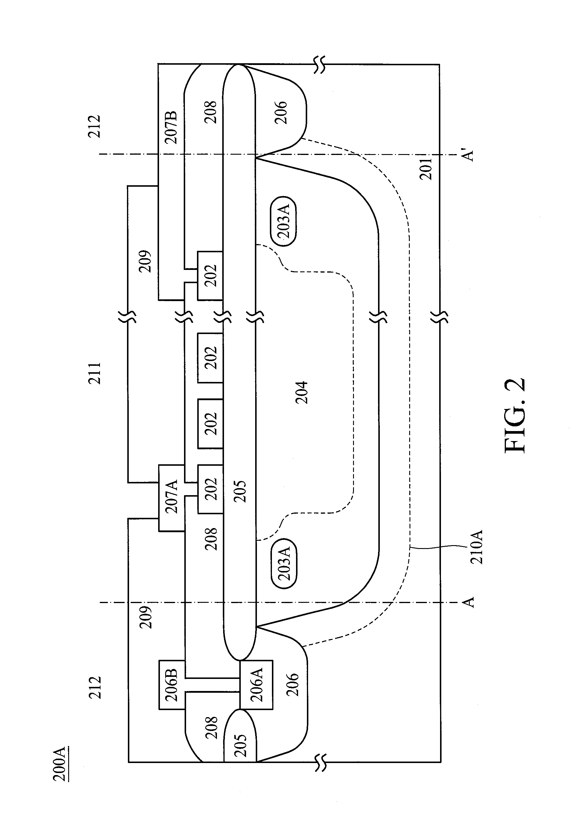
[0020]One embodiment of the present invention provides a structure depicted in FIG. 1. Shown in FIG. 1 is a top view of a semiconductor structure 10 with a high volt...


PUM


Abstract

A semiconductor structure with a high voltage area and a low voltage area includes a substrate of a first conductivity type accommodating the high voltage area and the low voltage area. A resistor is on the substrate, connecting the high voltage area and the low voltage area, and the resistor resides substantially in the high voltage area. The structure further includes a first doped region of the first conductivity type in the substrate between the high voltage area and the low voltage area, and a second doped region of a second conductivity type between the substrate and the first doped region. Moreover, an insulating layer is formed between the resistor and the first doped region.

Description

CROSS-REFERENCE TO RELATED APPLICATION[0001]This application claims the priority benefit of U.S. provisional application Ser. No. 61 / 778,577, filed on Mar. 13, 2013. The entirety of the above-mentioned patent application is hereby incorporated by reference herein and made a part of this specification.FIELD OF THE INVENTION[0002]The present invention relates in general to a semiconductor structure and more particularly to a semiconductor structure with a high voltage resistance.BACKGROUND[0003]High voltage integrated circuits (HVICs) translate low-voltage control signals to levels that are suitable for driving power switches in high voltage applications. HVICs can also translate signals from higher voltage levels to lower voltage levels in a single chip with high voltage and low voltage circuits, sharing the same I / O pad. As such, voltage isolation must be carefully managed to prevent the low voltage circuit from permanent damages caused by high stress. One of the HVIC designs is to ...

Claims


Application Information

Patent Timeline
IPC IPC(8): G05F3/02H01L49/02
CPCG05F3/02H01L27/0629H01L28/20H01L29/66113
Inventor LIN, CHEN-YUANCHAN, CHING-LINLIN, CHENG-CHILIEN, SHIH-CHIN
Owner MACRONIX INT CO LTD
Why Eureka
Try Eureka