

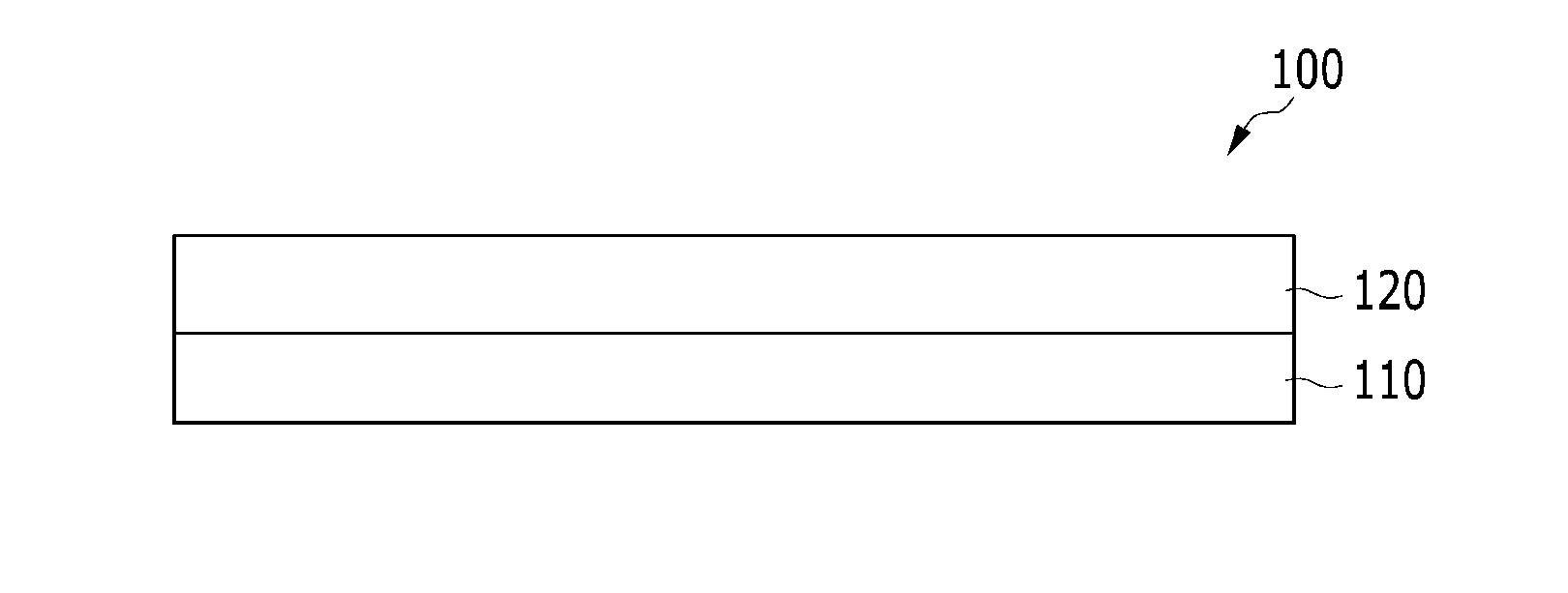
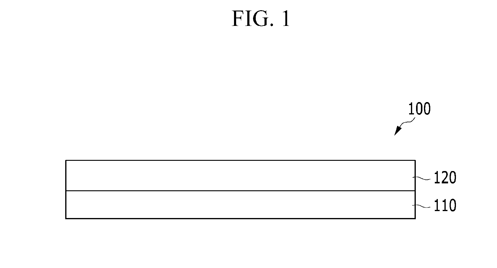
Compensation film, and optical film and display device including the same
a technology of compensating film and optical film, which is applied in the direction of instruments, polarising elements, optical elements, etc., can solve the problems of deteriorating the effect of conventional compensation film, weak viewing angle dependency, and deteriorating the visibility and contrast ratio, etc., and achieves strong viewing angle dependency
- Summary
- Abstract
- Description
- Claims
- Application Information
AI Technical Summary
Benefits of technology
Problems solved by technology
Method used
Image

Examples
preparation example 1
Preparation of First Retardation Layers (Layer A to Layer D)
[0133]A poly(styrene-co-methacrylic acid) film (T080, manufactured by TOYO STYRENE) having a thickness of 100 micrometers (μm) is elongated in one axial direction (using a tension tester manufactured by Toyoseiki) at about 125° C. at a ratio of about 100% to provide a first retardation layer (A) having in-plane retardation of 220 nm at reference wavelength (550 nm).
[0134]Further, a poly(styrene-co-methacrylic acid) film (T080, manufactured by TOYO STYRENE) having a thickness of 100 μm is elongated in one axial direction (using a tension tester manufactured by Toyoseiki) at about 125° C. at a ratio of about 120% to provide a first retardation layer (B) having in-plane retardation of 240 nm at reference wavelength (550 nm).
[0135]Further, a poly(styrene-co-methacrylic acid) film (T080, manufactured by TOYO STYRENE) having a thickness of 100 μm is elongated in one axial direction (using a tension tester manufactured by Toyoseik...
preparation example 2
Preparation of Second Retardation Layers (Layer E to Layer G)
[0137]A poly(styrene-co-methacrylic acid) film (T080, manufactured by TOYO STYRENE) having a thickness of 100 μm is elongated in one axial direction (using a tension tester manufactured by Toyoseiki) at about 135° C. at a ratio of about 60% to provide a second retardation layer (E) having in-plane retardation of 100 nm at reference wavelength (550 nm).
[0138]Further, a poly(styrene-co-methacrylic acid) film (T080, manufactured by TOYO STYRENE) having a thickness of 100 μm is elongated in one axial direction (using a tension tester manufactured by Toyoseiki) at about 135° C. at a ratio of about 75% to provide a second retardation layer (F) having in-plane retardation of 120 nm at reference wavelength (550 nm).
[0139]Further, a poly(styrene-co-methacrylic acid) film (T080, manufactured by TOYO STYRENE) having a thickness of 100 μm is elongated in one axial direction (using a tension tester manufactured by Toyoseiki) at about 1...
examples 1 to 8
Manufacturing of Compensation Films
[0140]The first retardation layers (A-D) according to Preparation Example 1 and the second retardation layers (E-G) according to Preparation Example 2 are assembled as described in Table 1 below to provide compensation films according to Examples 1 to 8.
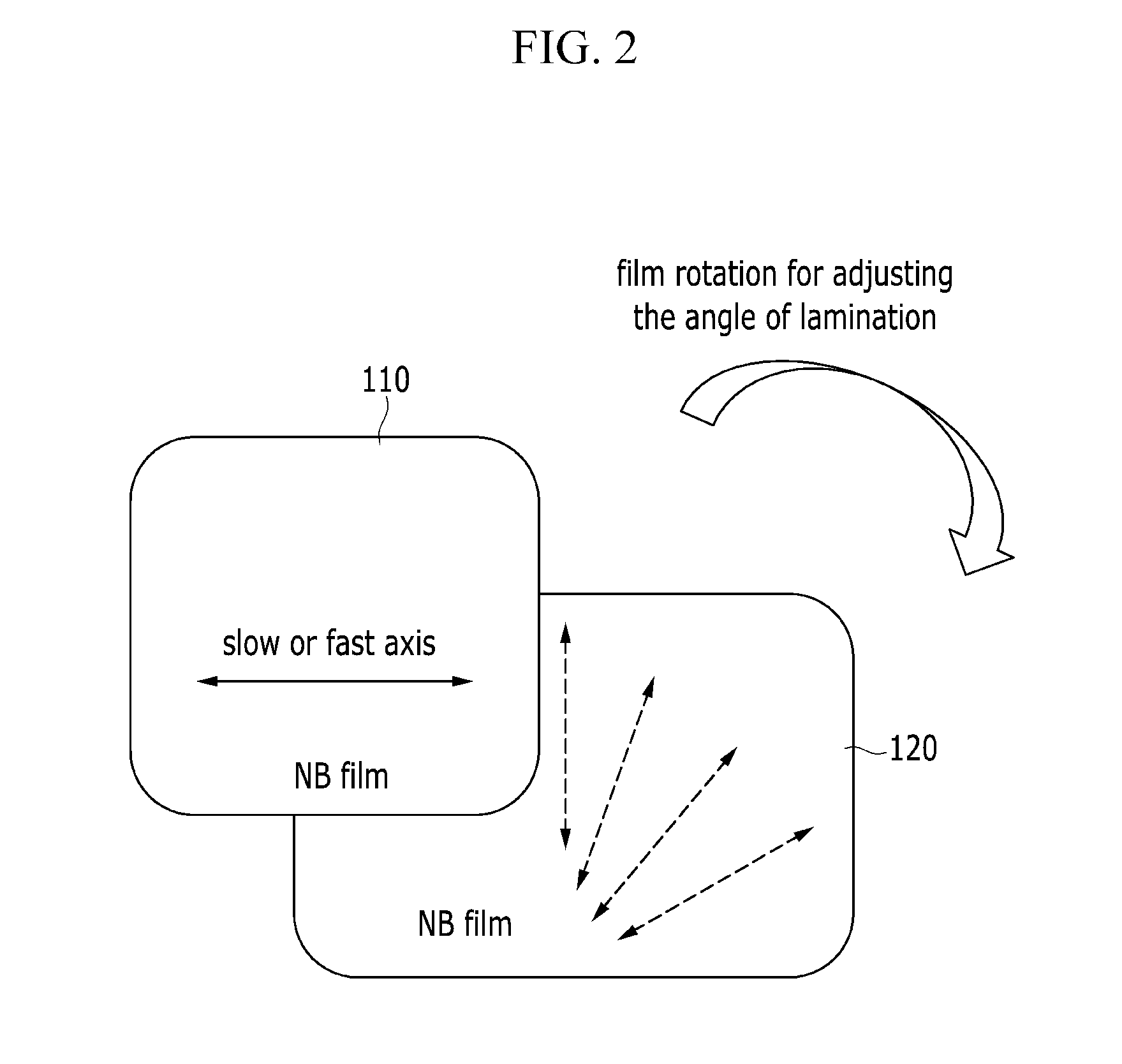
[0141]Particularly, a first retardation layer and a second retardation layer are assembled in pairs as described in Table 1 by disposing the second retardation layer below the first retardation layer to have a specific angle between the slow axes or the fast axes thereof from 0° to 90°. Subsequently, an adhesion film is transcribed on one side of either the first retardation layer or the second retardation layer, and then the releasing film attached to the other side of the adhesion film is removed to provide a compensation film assembled with the first retardation layer and the second retardation layer maintaining the specific angle between the slow axes or the fast axes thereof. The assembly of th...
PUM
| Property | Measurement | Unit |
|---|---|---|
| wavelengths | aaaaa | aaaaa |
| wavelengths | aaaaa | aaaaa |
| angle | aaaaa | aaaaa |
Abstract
Description
Claims
Application Information