Touch Display Device and Touch Display Panel

a display device and touch technology, applied in the direction of solid-state devices, semiconductor devices, instruments, etc., can solve the problems of difficult to fabricate compact touch display panels and complicated processes, and achieve the effect of improving the efficiency of display fabrication processing

Active Publication Date: 2019-05-02
LG DISPLAY CO LTD
View PDF6 Cites 6 Cited by
  • Summary
  • Abstract
  • Description
  • Claims
  • Application Information

AI Technical Summary

Benefits of technology

[0011]Various aspects of the present disclosure provide a touch display device and panel having a compact structure, by which the overall thickness can be reduced.
[0012]Also provided are a touch display device and panel having an improved data panel structure.
[0014]Exemplary embodiments according to the present disclosure may provide a touch display device and panel, the overall thickness of which is reduced, due to an insulating film being located on and in contact with an encapsulating layer of the display panel.
[0016]According to exemplary embodiments, the touch display device and panel can be easily fabricated, due to the simplified fabrication process of the touch display panel.
[0017]According to exemplary embodiments, the overall panel thickness of the touch display device and panel can be reduced.
[0018]According to exemplary embodiments, in the touch display device and panel, touch sensor metals may be used in a data pad part and a touch pad part to protect data link lines while reducing the difference in height between the data pad part and the touch pad part.

Problems solved by technology

In this case, the process may be more complicated, since the deposition of the buffer layer and the deposition of the insulating film are repeatedly performed.
In addition, since the buffer layer remaining in the structure of the display panel increases the overall thickness of the touch display panel, to which a variety of structures, such as touch electrodes, must be added, it may be difficult to fabricate a compact touch display panel.

Method used


Image

  • Touch Display Device and Touch Display Panel
  • Touch Display Device and Touch Display Panel
  • Touch Display Device and Touch Display Panel

Examples


Embodiment Construction

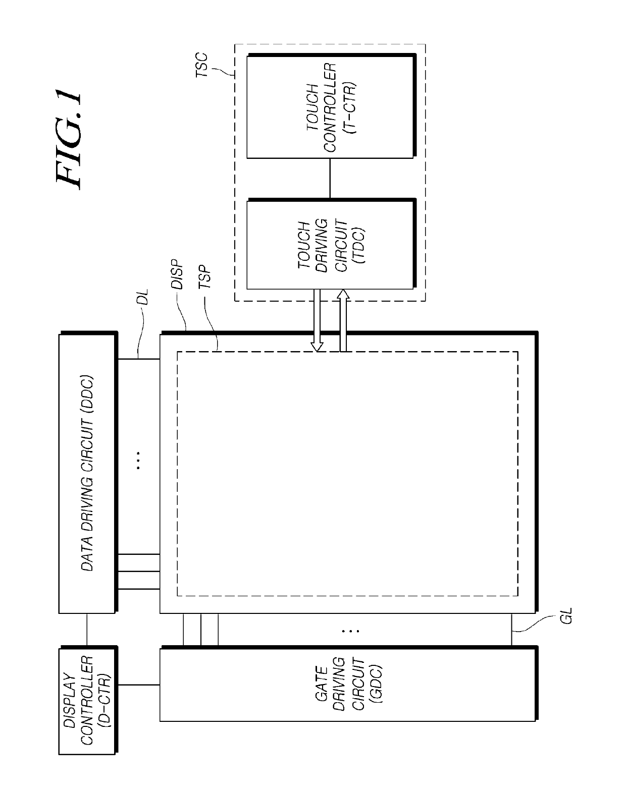
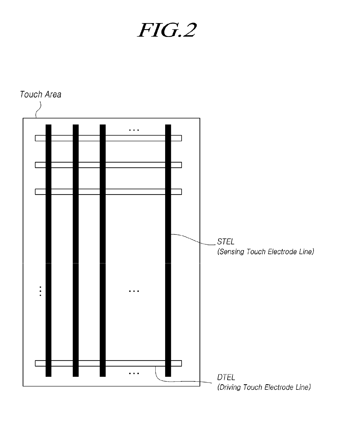
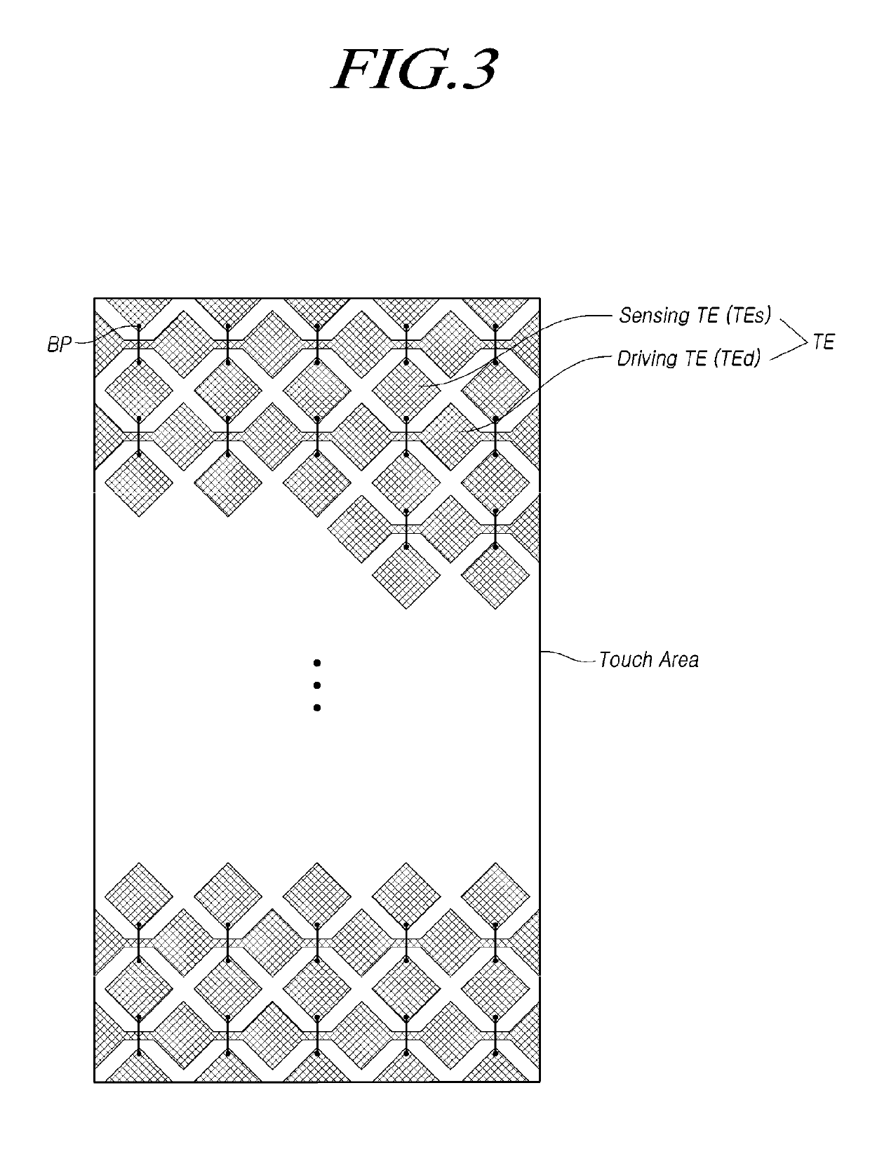
[0037]Hereinafter, reference will be made to embodiments of the present disclosure in detail, examples of which are illustrated in the accompanying drawings. Throughout this document, reference should be made to the drawings, in which the same reference numerals and symbols will be used to designate the same or like components. In the following description of the present disclosure, detailed descriptions of known functions and components incorporated herein will be omitted in the case that the subject matter of the present disclosure may be rendered unclear thereby.

[0038]It will also be understood that, while terms such as “first,”“second,”“A,”“B,”“(a),” and “(b)” may be used herein to describe various elements, such terms are merely used to distinguish one element from other elements. The substance, sequence, order, or number of such elements is not limited by these terms. It will be understood that when an element is referred to as being “connected to” or “coupled to” another elem...


PUM


Abstract

A touch display device and panel. In the display panel, an insulating film is provided on and in contact with an encapsulating layer, thereby reducing the entire thickness of the panel. The fabrication process of the touch display panel is simplified, thereby facilitating fabrication of the touch display device and panel.

Description

CROSS-REFERENCE TO RELATED APPLICATION[0001]This application claims priority to Republic of Korea Patent Application No. 10-2017-0141565, filed on Oct. 27, 2017, which is hereby incorporated by reference in its entirety.BACKGROUNDField of Disclosure[0002]Exemplary embodiments of the present disclosure relate to a touch display device and panel.Description of Related Art[0003]In response to the development of the information society, demand for a variety of display devices for displaying images is increasing. In this regard, a range of display devices, such as liquid crystal display (LCD) devices, plasma display devices, and organic light-emitting diode (OLED) display devices, have recently come into widespread use.[0004]Among such display devices, touch display devices provide touch-based user interfaces enabling users to intuitively and conveniently input data or instructions directly to devices, rather than using conventional data input systems, such as buttons, a keyboard, or a m...

Claims


Application Information

Patent Timeline
Patent Type & Authority Applications(United States)
IPC IPC(8): G06F3/041H01L51/52G06F3/044G06F3/047H01L27/32
CPCG06F3/0412H01L51/5237G06F3/044G06F3/047H01L27/3276H01L27/3246G06F3/0416G06F2203/04112G06F3/0448G06F3/041G06F3/0443G06F3/0446G06F3/04164H10K59/40H10K59/35H10K50/84H10K59/124H10K59/122H10K59/131
Inventor HWANG, KWANGJOAN, SUCHANGLEE, YANGSIKLEE, DEUKSU
Owner LG DISPLAY CO LTD
Why Eureka
Try Eureka