Thin film transistor array substrate for digital x-ray detector device and digital x-ray detector device including the same

Active Publication Date: 2021-06-24
LG DISPLAY CO LTD
View PDF0 Cites 0 Cited by
  • Summary
  • Abstract
  • Description
  • Claims
  • Application Information

AI Technical Summary

Benefits of technology

The present disclosure provides a thin film transistor array substrate and a digital X-ray detector device that can minimize defects caused by static electricity and signal interference. This means that the device can reduce the likelihood of defects and noise in the readout circuit signal. Additionally, the invention is also about minimizing defects caused by static electricity introduced into the readout circuit pad or readout line.

Problems solved by technology

Thus, it takes a long time to check the result.
Especially, in the film printing scheme, there are some difficulties in storing and preserving the printed film.
Defects of elements may occur based on static electricity introduced into the elements because the elements are susceptible to electric shock such as static electricity introduced from outside.
In some cases where the display device includes the ESD prevention circuit at the readout line or the connection line between the readout circuit pad and the driving area, noise may occur in a readout signal value due to signal interference.
Therefore, the digital X-ray detector device may not include the ESD prevention circuit.
In some cases where the display device may not include the ESD prevention circuit in the readout circuit pad area to avoid the signal interference, defects of the elements caused by the static electricity introduced through the readout circuit pad area may not be solved.

Method used


Image

  • Thin film transistor array substrate for digital x-ray detector device and digital x-ray detector device including the same
  • Thin film transistor array substrate for digital x-ray detector device and digital x-ray detector device including the same
  • Thin film transistor array substrate for digital x-ray detector device and digital x-ray detector device including the same

Examples


Embodiment Construction

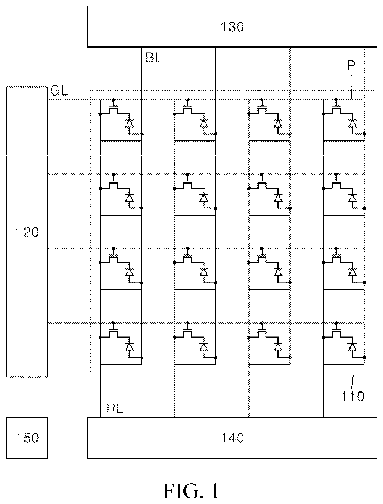
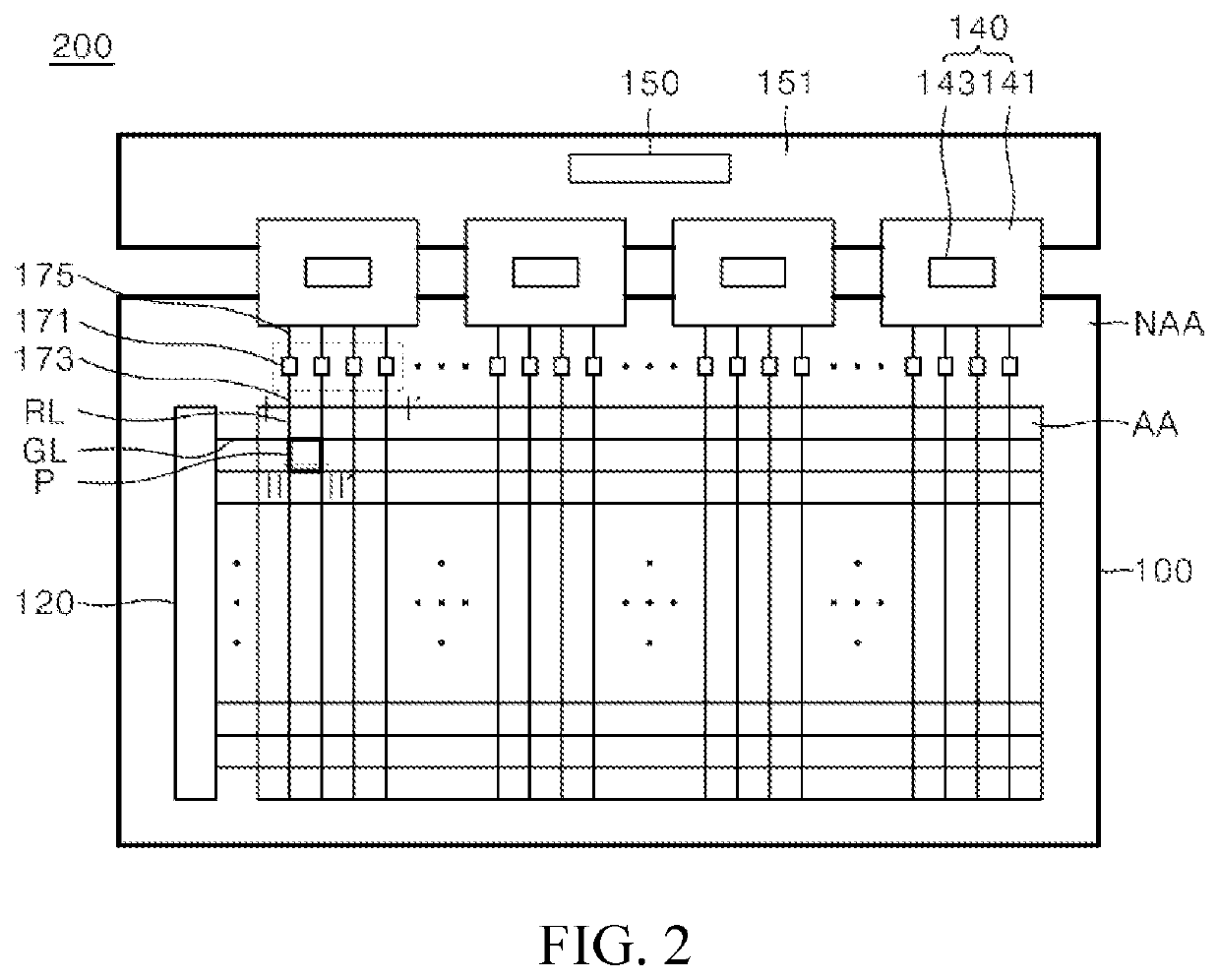
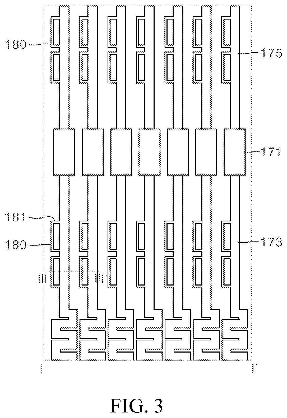
[0041]Some aspects of the present disclosure are described in detail with reference to the accompanying drawings. Accordingly, the skilled person in the art to which the present disclosure pertains may easily implement the technical idea of the present disclosure. In the description of the present disclosure, if it is determined that a detailed description of a well-known technology relating to the present disclosure may be omitted if it unnecessarily obscures the gist of the present disclosure. One or more aspects of the present disclosure are described in detail with reference to the accompanying drawings. In the drawings, same reference numerals may be used to refer to same or similar components.

[0042]In this document, the terms “upper,”“lower,”“on,”“under,” or the like are used such that, where a first component is arranged at “an upper portion” or “a lower portion” of a second component, the first component may be arranged in contact with the upper surface (or the lower surface...


PUM


Abstract

A thin film transistor array substrate for a digital X-ray detector device includes a base substrate where a driving area and a non-driving area are defined; at least one readout circuit pad disposed in the non-driving area and electrically connected to the drive area; at least one readout circuit pad connection line electrically connecting the driving area to the at least one readout circuit pad; and at least one electrostatic induction line electrically connected to the at least one readout circuit pad connection line, wherein the at least one electrostatic induction line has a greater resistance than a resistance of the at least one readout circuit pad connection line.

Description

CROSS REFERENCE TO RELATED APPLICATION[0001]The present disclosure claims priority to and the benefit of Korean Patent Application No. 10-2019-0171496, filed on Dec. 20, 2019, the disclosure of which is incorporated herein by reference in its entirety.BACKGROUNDField of the Disclosure[0002]The present disclosure relates to a thin film transistor array substrate for a digital X-ray detector device capable of minimizing a defect due to an inflow of static electricity and the digital X-ray detector device including the same.Description of the Background[0003]Because X-ray is of a short wavelength, the X-ray may pass through an object easily. The transmittance of the X-ray depends on an inner density of the object. Therefore, an internal structure of the object may be observed by detecting an amount of the X-ray transmitted through the object.[0004]One of X-ray based inspection methods used in a medical field is a film printing scheme. However, in the film printing scheme, to check a re...

Claims


Application Information

Patent Timeline
IPC IPC(8): H01L27/146G01T1/20
CPCH01L27/14636G01T1/20184H01L27/14663H01L27/0288G01T1/246G01T1/247G01T1/2018G01T1/161H01L27/14612H01L27/1214G01T1/24G01T1/1617G01T1/1618H10K39/36
Inventor KONG, MINSUKKIM, SOYOUNGKANG, MOONSOOYOON, JAEHO
Owner LG DISPLAY CO LTD
Why Eureka
Try Eureka