Modification of selectivity for sensing for nanostructure device arrays

a nanostructure device and selectivity technology, applied in the field of system for detecting and identifying chemical species, can solve the problems of long recovery time of solid-state sensors, poor reproducibility, and limited variety of detection results

Inactive Publication Date: 2005-06-14
NANOMIX INC
View PDF21 Cites 117 Cited by
  • Summary
  • Abstract
  • Description
  • Claims
  • Application Information

AI Technical Summary

Problems solved by technology

Solid state sensors have long recovery times, poor reproducibility, and can detect only a limited variety of chemical species.
Solid state sensors are limited by their lack of sensitivity to certain chemical species and by their non-linear response.
However, the gas chromatographic approach requires a significant amount of time for all chemical species to be detected, as they must be detected serially, which is very time-consuming.
Furthermore, systems of this type are not small enough for many field applications.

Method used


Image

  • Modification of selectivity for sensing for nanostructure device arrays
  • Modification of selectivity for sensing for nanostructure device arrays
  • Modification of selectivity for sensing for nanostructure device arrays

Examples


Embodiment Construction

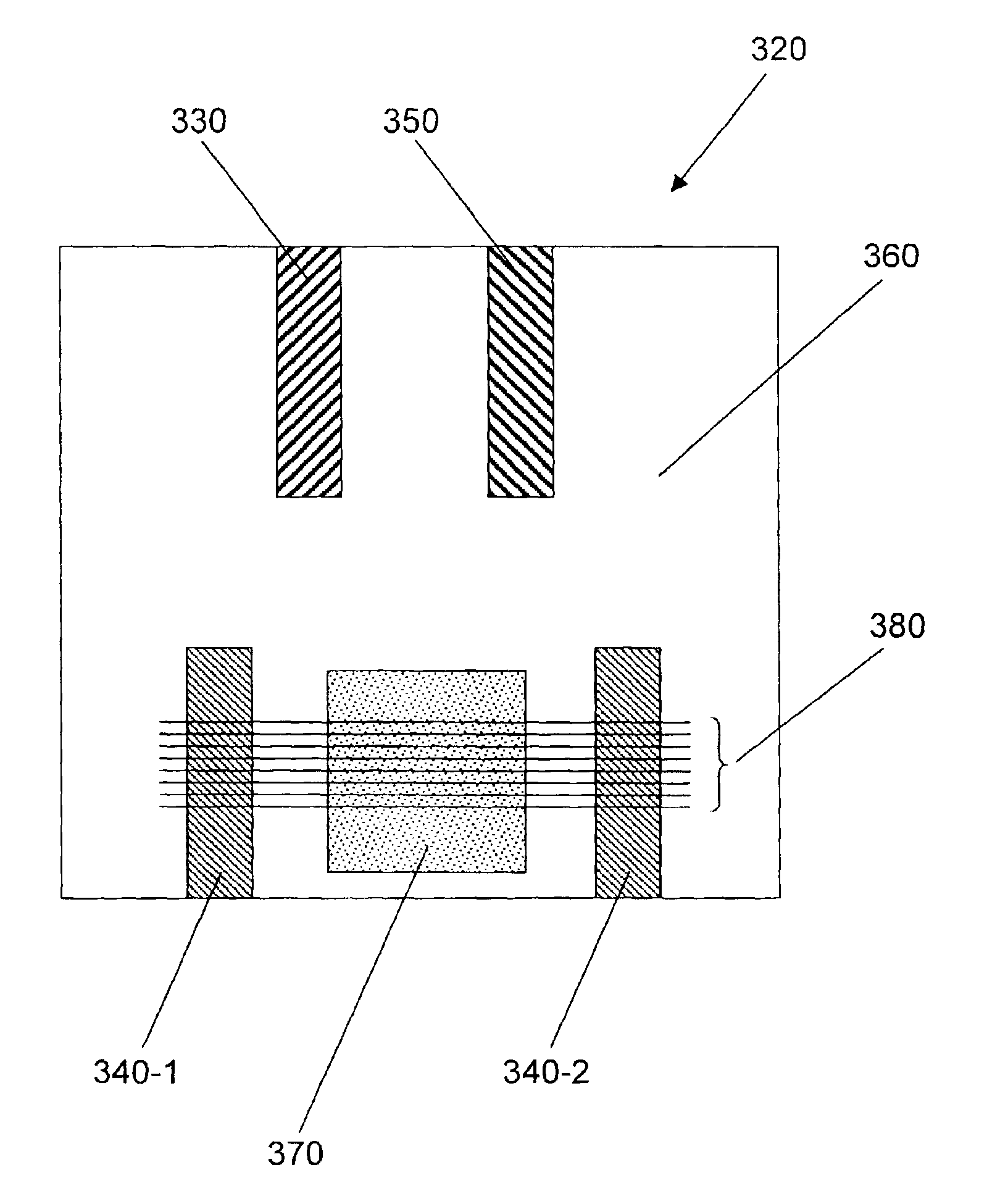
[0041]Recently, nanostructures have attracted attention as sensor components. Coating of nanotubes to make nanostructure sensing devices has been described by Zhang et al. in Chemical Physics Letters 331 (2000), p. 35 and by Zhang et al. in Applied Physics Letters 77 (2000), p. 3015. Nanostructure sensing devices show great promise for many applications. They can be made very small; even an array with a large number of nanostructure sensing devices can be made very small. They can be modified to detect a wide variety of chemical species. They use very little power. But in general, nanostructure sensing devices have been made only in small quantities for lab testing, and the techniques for producing nanostructure sensing devices have not been developed for large-scale manufacturing.

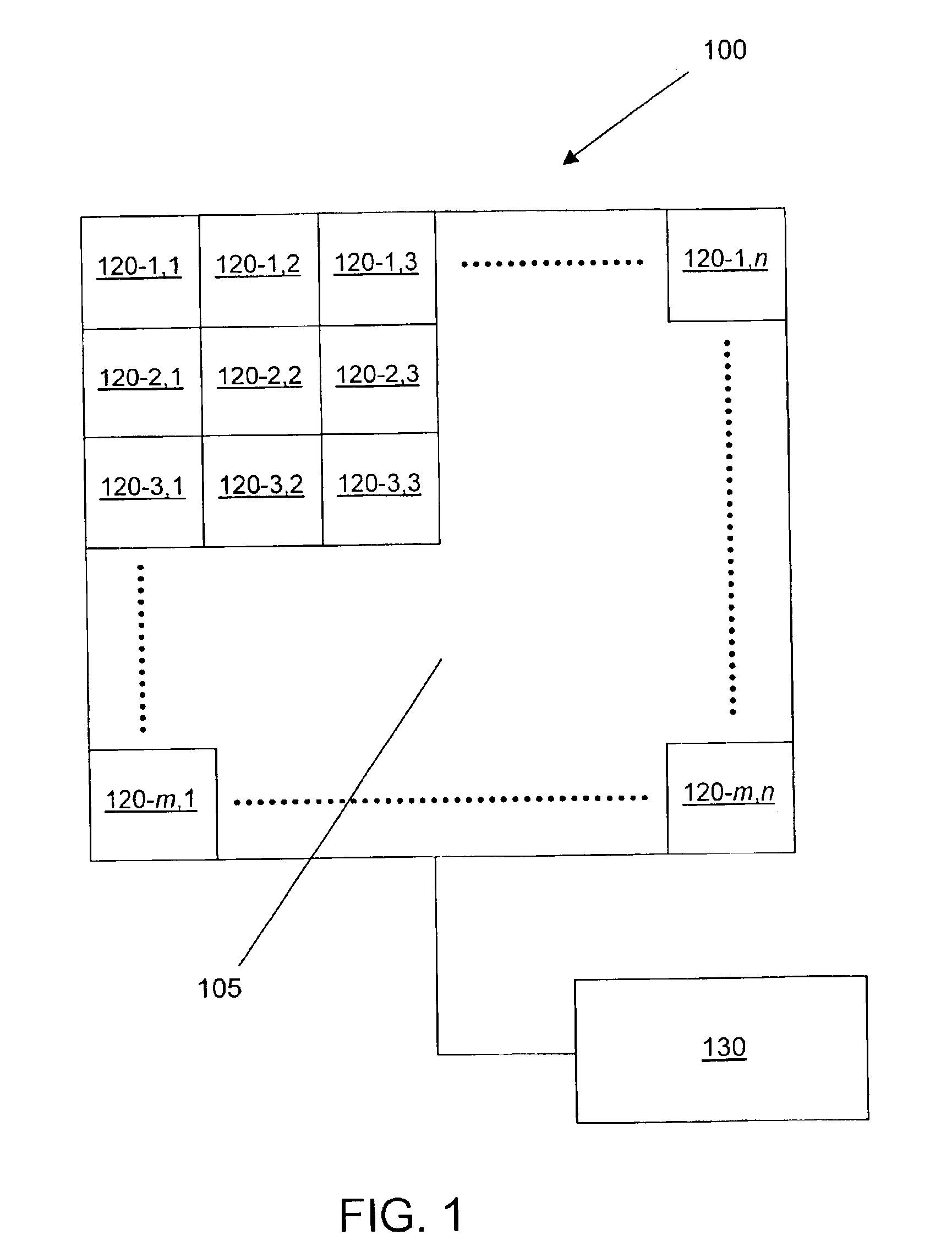
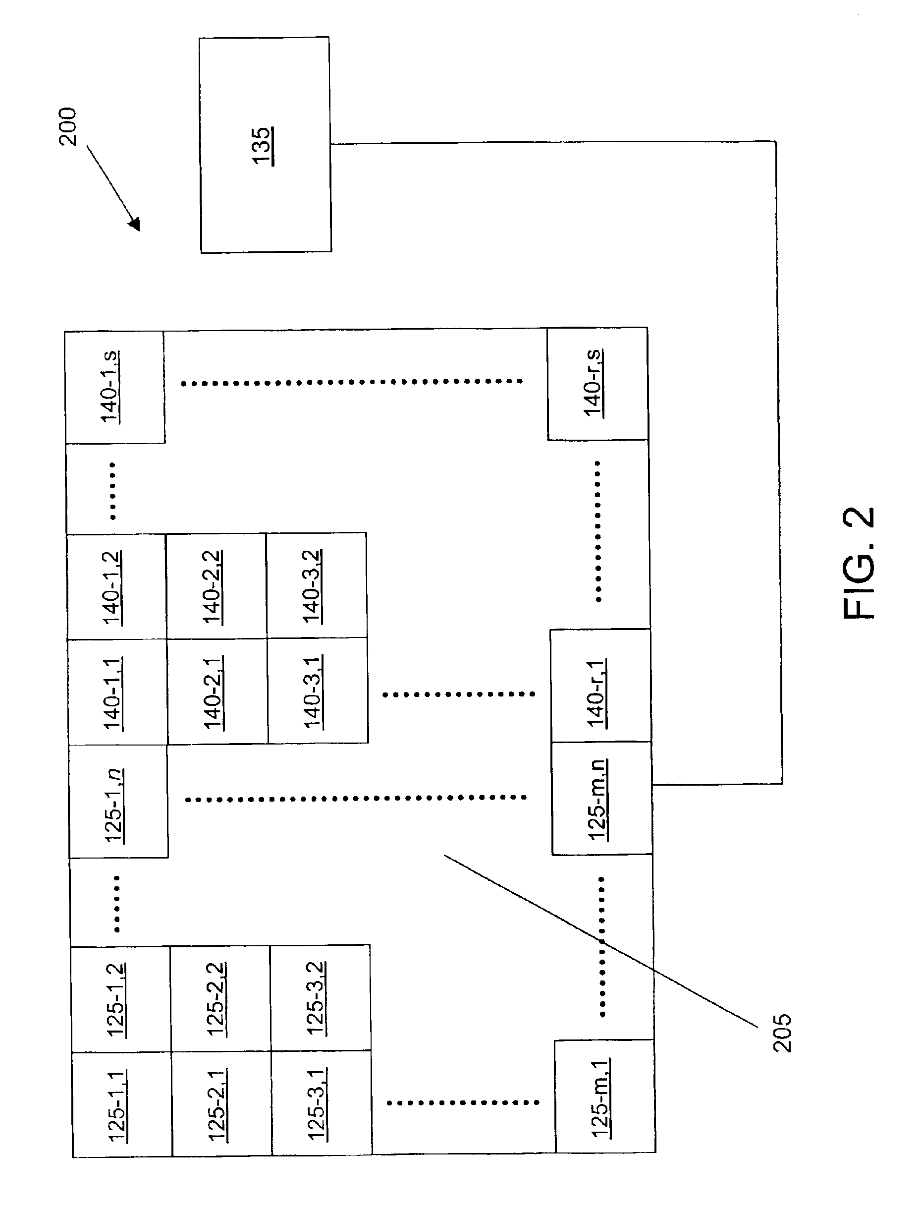
[0042]The embodiments of the present invention are illustrated in the context of using an array of nanostructure sensing devices to detect a plurality of chemical or biological species. The skilled artisan...


PUM

PropertyMeasurementUnit
frequencyaaaaaaaaaa
frequencyaaaaaaaaaa
hydrophobicaaaaaaaaaa

Abstract

An electronic system for selectively detecting and identifying a plurality of chemical species, which comprises an array of nanostructure sensing devices, is disclosed. Within the array, there are at least two different selectivities for sensing among the nanostructure sensing devices. Methods for fabricating the electronic system are also disclosed. The methods involve modifiying nanostructures within the devices to have different selectivity for sensing chemical species. Modification can involve chemical, electrochemical, and self-limiting point defect reactions. Reactants for these reactions can be supplied using a bath method or a chemical jet method. Methods for using the arrays of nanostructure sensing devices to detect and identify a plurality of chemical species are also provided. The methods involve comparing signals from nanostructure sensing devices that have not been exposed to the chemical species of interest with signals from nanostructure sensing devices that have been exposed to the chemical species of interest. Nanostructure sensing device array structures that can measure and subtract out environmental factors are also disclosed.

Description

DOMESTIC PRIORITY CLAIM[0001]This application repeats a substantial portion of prior application Ser. No. 10 / 099,664, filed Mar. 15, 2002, and adds and claims additional disclosure not presented in the prior application. Since this application names an inventor or inventors named in the prior application, it is a continuation-in-part of the prior application. The priority of U.S. Provisional Application No. 60 / 366,566, filed Mar. 22, 2002, is also claimed.BACKGROUND OF THE INVENTION[0002]1. Field of the Invention[0003]This invention relates generally to a system for detecting and identifying chemical species and, more particularly, to a system that uses an array of nanostructure sensing devices, which have been modified for selectivity for sensing a plurality of chemical species and methods of fabricating the same.[0004]2. Description of the Related Art[0005]Chemical and biological sensing is important in many industrial, medical, agricultural, and environmental monitoring applicati...

Claims


Application Information

Patent Timeline
Patent Type & Authority Patents(United States)
IPC IPC(8): G01N15/06G01N31/22G01N33/00G01N21/00G01N35/00H01C7/00B01L3/00C12QG01N27/12G01N33/48
CPCB82Y15/00G01N27/126G01N27/127B01J2219/00653B01L3/5027Y10T436/11Y10S977/957Y10S977/84Y10S977/958Y10S977/882Y10S977/855Y10S977/92
Inventor GABRIEL, JEAN-CHRISTOPHE P.COLLINS, PHILIP G.BRADLEY, KEITHGRUNER, GEORGE
Owner NANOMIX INC
Why Eureka
Try Eureka