Plasma pre-treating surfaces for atomic layer deposition

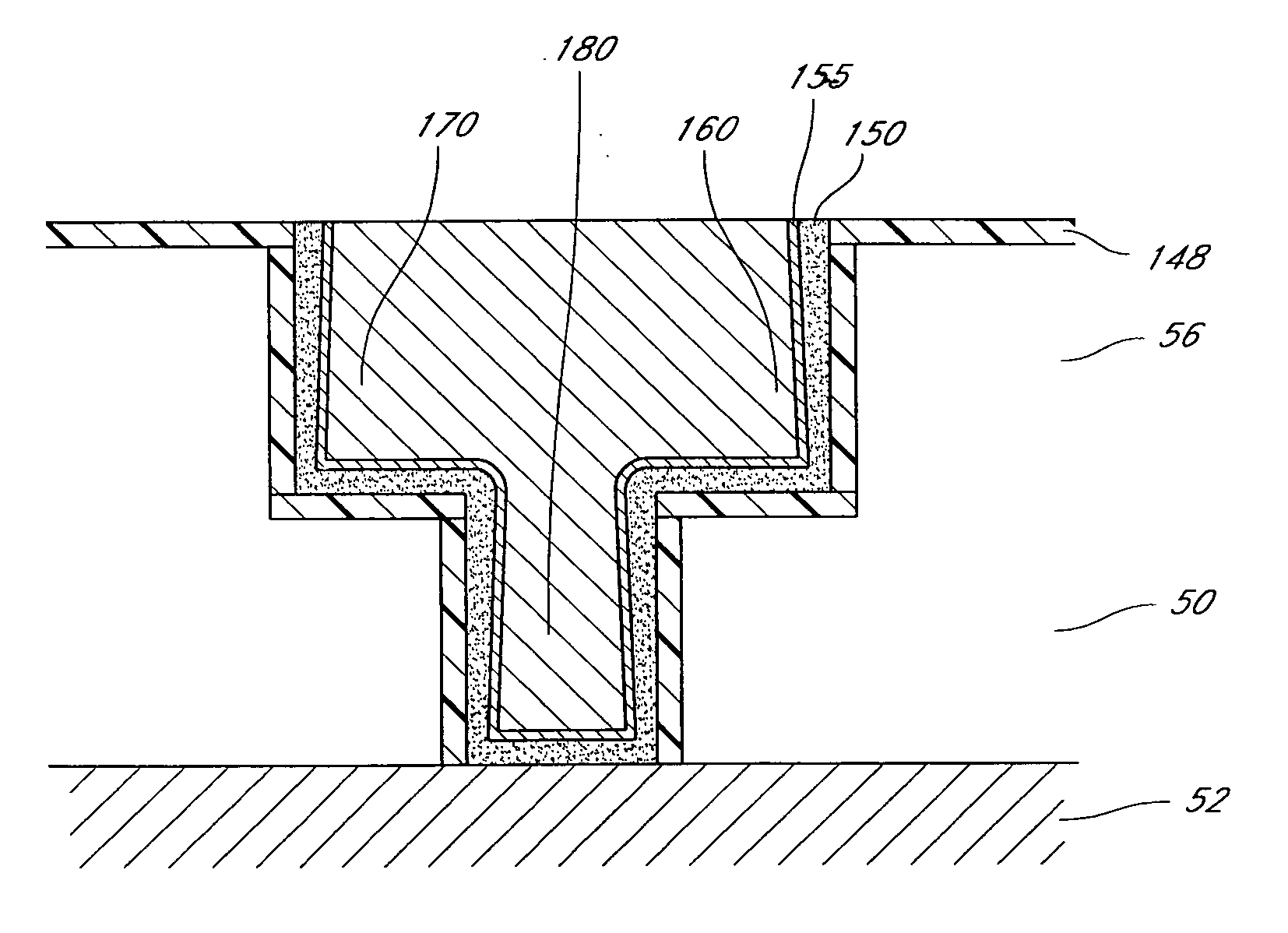
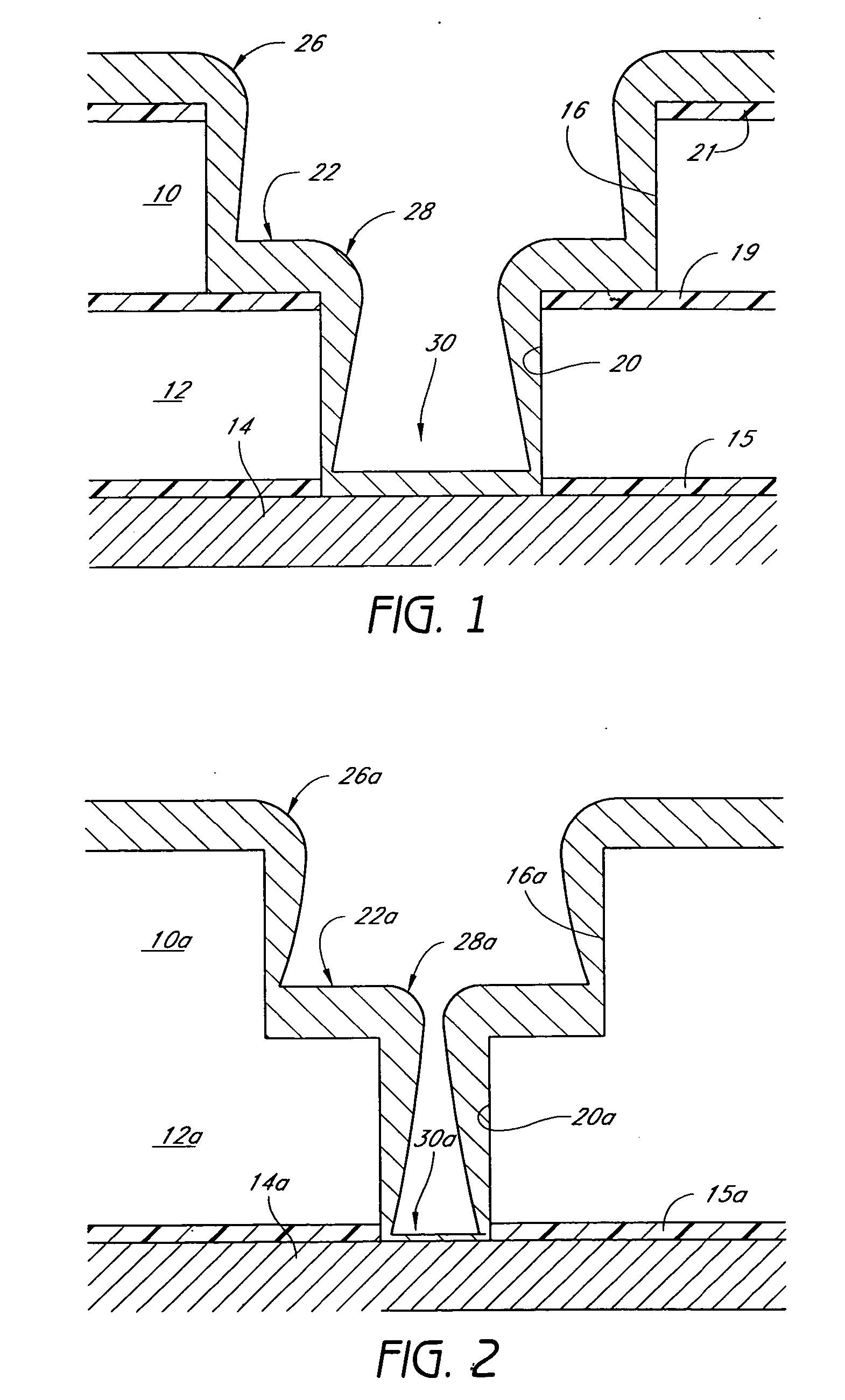
a technology of atomic layer and surface treatment, which is applied in the direction of vacuum evaporation coating, semiconductor/solid-state device details, coatings, etc., can solve the problems of unfavorable short circuit between devices and lines, difficulty in completely filling deep, narrow openings with conductive materials, and difficulty in conformal deposition of liners b>22/b>, and achieve the effect of improving the barrier property and the barrier property of the barrier layer associated

Active Publication Date: 2006-09-28
ASM IP HLDG BV
View PDF52 Cites 79 Cited by
  • Summary
  • Abstract
  • Description
  • Claims
  • Application Information

AI Technical Summary

Benefits of technology

[0039] Another aspect of the invention comprises a damascene metallization process. The process comprises forming a trench in a porous insulating layer above a semiconductor substrate, forming a contact via extending downwardly from a floor of the trench to expose at least part of an underlying conductive element, treating the exposed part of the underlying conductive element with an oxide removal process to reduce any oxidized metal, t

Problems solved by technology

In addition to providing insulating layers around such conductive elements, care must be taken to prevent diffusion and spiking of conductive materials through the insulating layers, which can cause undesired short circuits among devices and lines.
Completely filling deep, narrow openings with conductive material is becoming ever more challenging as integrated circuit dimensions are constantly scaled down in pursuit of faster operational processing speeds and lower power consumption.
Conformal deposition of the liners 22, however, is very difficult with conventional processing.
Unfortunately, PVD of metal into high aspect ratio voids necessitates much greater deposition on the top surfaces of the workpiece to produce adequate coverage of the via bottom.
This poor step coverage is a result of the high aspect ratio of voids formed for dual damascene processing in today's integrated circuits.
Conventional deposition processes produce very poor step coverage (i.e., the ratio of sidewall coverage to field or horizontal surface coverage) of such high aspect ratio vias for a variety of reasons.
Although PVD deposition can be directed more specifically to the via bottom, e.g., by collimation or by ionization of the depositing vapor, such additional directionality tends to sacrifice sidewall coverage.
S

Method used


Image

  • Plasma pre-treating surfaces for atomic layer deposition
  • Plasma pre-treating surfaces for atomic layer deposition
  • Plasma pre-treating surfaces for atomic layer deposition

Examples


examples

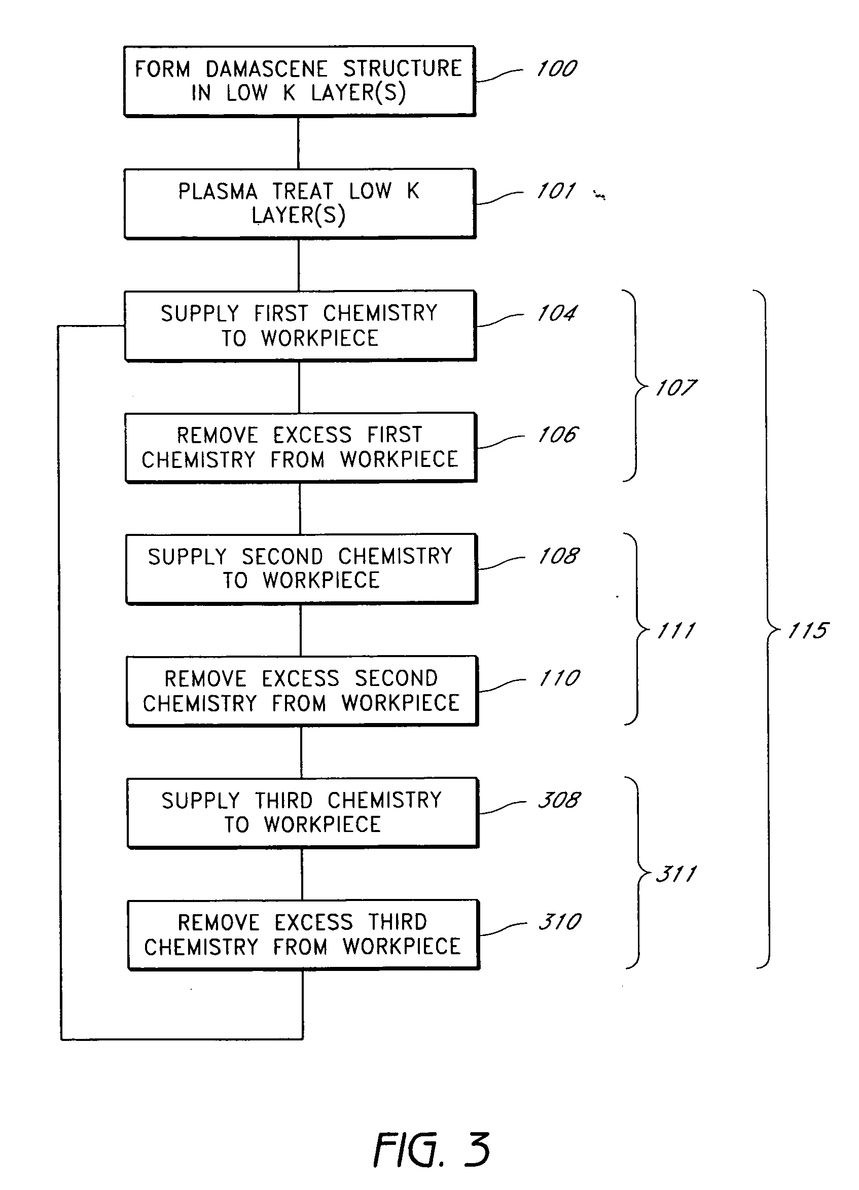
[0137] The description below provide exemplary process recipes for forming metal nitride layers suitable for barrier applications in dual damascene metallization schemes for integrated processing. The process recipes represents one cycle in a single-wafer process module. In particular, the illustrated parameters are developed for use in the single-wafer ALD module commercially available under the trade name Pulsar 3000™ from ASM America, Inc., Phoenix Ariz.

[0138] Note that the parameters in the tables below are exemplary only. Each process phase is desirably arranged to saturate the via and trench surfaces, and more particularly to saturate the plasma treated surface of the insulating layer. Purge steps are arranged to remove reactants between reactive phases from the substrate. The examples herein can be conducted upon planar, unpatterned wafer surfaces in a POLYGON™ cluster tool available from ASM International, N.V. of Bilthoven, the Netherlands. Similar ALD processes have been ...


PUM

PropertyMeasurementUnit
Temperatureaaaaaaaaaa
Fractionaaaaaaaaaa
Fractionaaaaaaaaaa

Abstract

Method and structures are provided for conformal lining of dual damascene structures in integrated circuits. Preferred embodiments are directed to providing conformal lining over openings formed in porous materials. Trenches are formed in, preferably, insulating layers. The layers are then adequately treated with a particular plasma process. Following this plasma treatment a self-limiting, self-saturating atomic layer deposition (ALD) reaction can occur without significantly filling the pores forming improved interconnects.

Description

RELATED APPLICATIONS [0001] The present application claims priority to U.S. Provisional Application No. 60 / 655,610, filed on Feb. 22, 2005, incorporated by reference in its entirety.FIELD OF THE INVENTION [0002] The invention relates generally to the treatment of a surface prior to atomic layer deposition (ALD). More particularly, the invention relates to plasma treating a layer prior to high conformality ALD layers over damascene structures in integrated circuits. BACKGROUND OF THE INVENTION [0003] When fabricating integrated circuits, layers of insulating, conducting, and semiconducting materials are deposited and patterned to produce desired structures. Interconnect “back end” metallization processes include via formation and metal line or wire formation. Via formation vertically connects conductive layers through an insulating layer. Conventionally, contact vias or openings are formed in the insulating layer, such as, PECVD deposited oxide (k=4) formed from tetraethylorthosilica...

Claims


Application Information

Patent Timeline
IPC IPC(8): H01L21/4763H01L21/44
CPCC23C14/02C23C16/02C23C16/36C23C16/45525C23C16/45531H01L21/02063H01L21/28562H01L21/3105H01L21/76807H01L21/7681H01L21/76826H01L21/76831H01L21/76843H01L21/76846H01L21/76873H01L21/28
Inventor KUMAR, DEVENDRAGOUNDAR, KAMAL KISHOREKEMELING, NATHANAEL R.C.FUKUDA, HIDEAKISPREY, HESSELSTOKHOF, MAARTEN
Owner ASM IP HLDG BV
Why Eureka
Try Eureka