Triple alignment substrate method and structure for packaging devices

a substrate and three-dimensional alignment technology, applied in the field of packaging techniques, can solve the problems of difficult to make larger, low yield of liquid crystal panels, and large volume of crts, and achieve the effects of improving integrated structure, convenient use, and high device yield

Active Publication Date: 2006-11-30
MIRADIA INC
View PDF2 Cites 77 Cited by
  • Summary
  • Abstract
  • Description
  • Claims
  • Application Information

AI Technical Summary

Benefits of technology

[0012] Many benefits are achieved by way of the present invention over conventional techniques. For example, the present technique provides an easy to use process that relies upon conventional technology. In some embodiments, the method provides higher device yields for the bonded substrates. Additionally, the method provides a process that is compatible with conventional process technology without substantial modifications to conventional equipment and processes. Preferably, the invention provides for an improved integrated structure including integrated circuits and mirror structures for display applications. In preferred embodiments, the present method provides a batch process, which can produce high throughput ...

Problems solved by technology

Although very successful, CRTs were often bulky, difficult to make larger, and had other limitations.
Unfortunately, liquid crystal panels often had low yields and were difficult to scale up to larger sizes.
These LCDs were often unsuitable for larger displays often required for television sets and the...

Method used


Image

  • Triple alignment substrate method and structure for packaging devices
  • Triple alignment substrate method and structure for packaging devices
  • Triple alignment substrate method and structure for packaging devices

Examples


Embodiment Construction

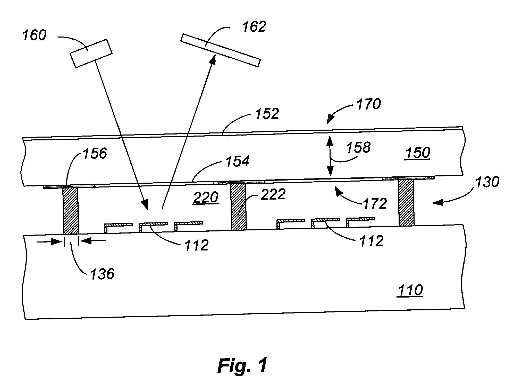
[0024] According to the present invention, techniques for packaging devices are provided. More particularly, the invention includes a method and structure for aligning and packaging optical devices. Merely by way of example, the invention has been applied to the alignment and bonding of substrates to form a composite substrate package. But it would be recognized that the invention has a much broader range of applicability.

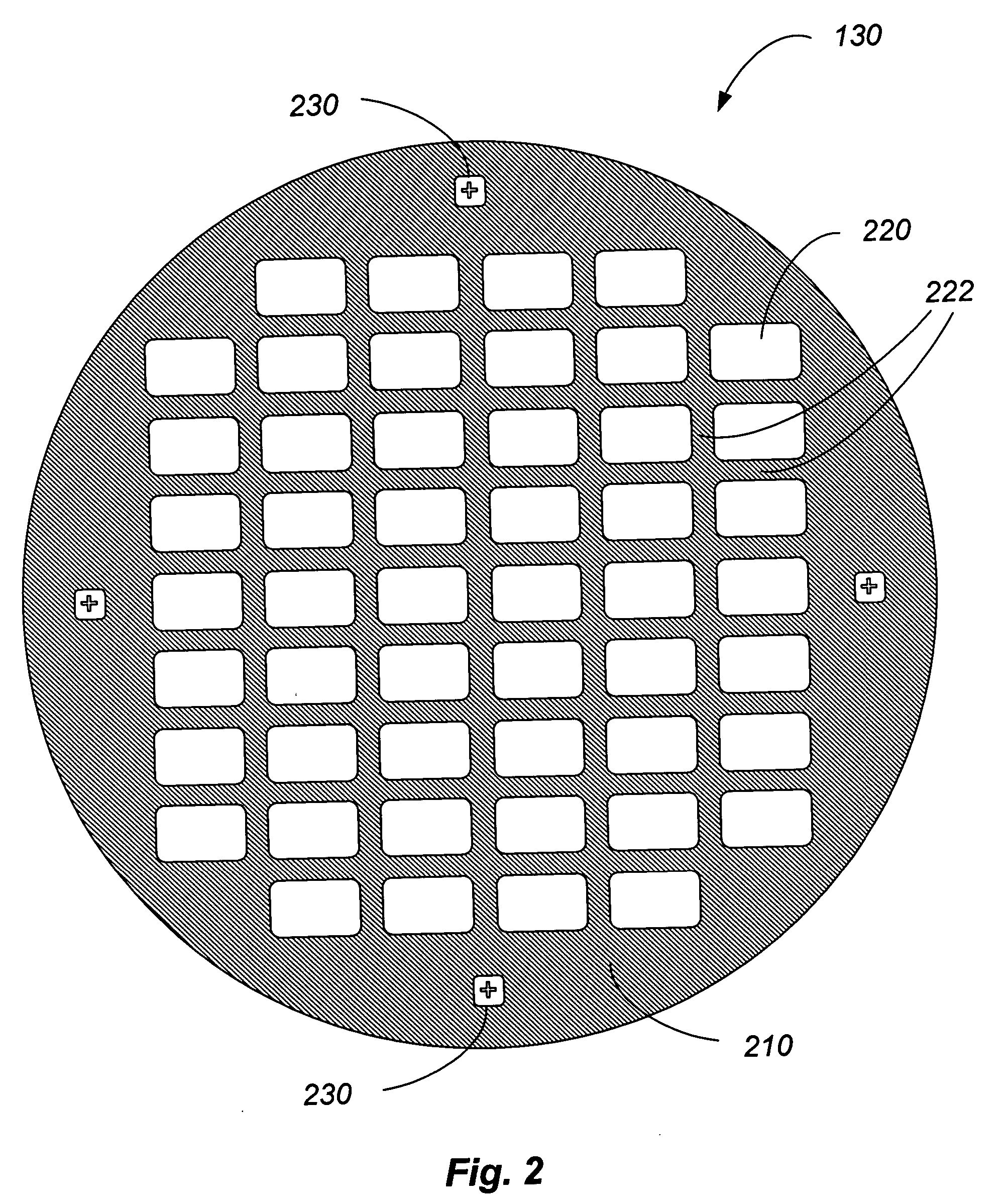
[0025]FIG. 1 is a simplified schematic cross-sectional diagram illustrating a composite substrate package according to an embodiment of the present invention. As illustrated in FIG. 1, a device substrate 110, a spacer structure 130, and a handle substrate 150 are joined by a bonding process to form a composite substrate structure. In some embodiments, the handle substrate is a transparent substrate. In the embodiment illustrated in FIG. 1, a number of MEMS devices 112 are arrayed on a surface of the device substrate. In one embodiment, the MEMS devices includes an...


PUM


Abstract

A method for aligning multiple substrates. The method includes providing a handle substrate, providing a spacer substrate, and forming a plurality of first alignment marks on a first surface of the handle substrate. The method also includes forming a plurality of self-limiting alignment marks on a first surface of the spacer substrate and forming a plurality of openings in the spacer substrate, each of the plurality of openings surrounded by standoff regions. The method further includes aligning the first surface of the handle substrate and the first surface of the spacer substrate using the first alignment marks and the self-limiting alignment marks and bonding the handle substrate to the spacer substrate to form a composite substrate structure. In a specific embodiment, the plurality of self-limiting alignment marks and the plurality of openings are formed using an anisotropic wet etching process that preferentially etches the spacer substrate.

Description

BACKGROUND OF THE INVENTION [0001] The present invention relates generally to packaging techniques. More particularly, the invention includes a method and structure for aligning and packaging optical devices. Merely by way of example, the invention has been applied to the alignment and bonding of substrates to form a composite substrate package. But it would be recognized that the invention has a much broader range of applicability. [0002] Visual display technologies have rapidly developed over the years. Most particularly, electronic displays for outputting television shows, streaming video, and the like. From the early days, cathode ray tube technology, commonly called CRTs, outputted selected pixel elements onto a glass screen in conventional television sets. These television sets originally output black and white moving pictures. Color television sets soon replaced most if not all black and white television units. Although very successful, CRTs were often bulky, difficult to mak...

Claims


Application Information

Patent Timeline
IPC IPC(8): H01L33/00H01L21/76H01L21/30
CPCB81C3/002B81C2203/051G02B26/0833H01L2223/54453H01L23/544H01L2223/54426H01L21/30608H01L2924/0002H01L2924/00
Inventor YANG, XIAO
Owner MIRADIA INC
Why Eureka
Try Eureka