
AC/DC flyback converter
a converter and input current technology, applied in the field of improved single-stage inputcurrent shaping flyback converters, can solve the problems of increasing line current harmonics, reducing input power factor and reducing total harmonic distortion (thd), and reducing input power factor and reducing thd as much as their two-stage counterparts, so as to reduce input-current ripple, reduce conduction losses, and reduce input-current ripple
- Summary
- Abstract
- Description
- Claims
- Application Information
AI Technical Summary
Benefits of technology
Problems solved by technology
Method used
Image

Examples
Embodiment Construction
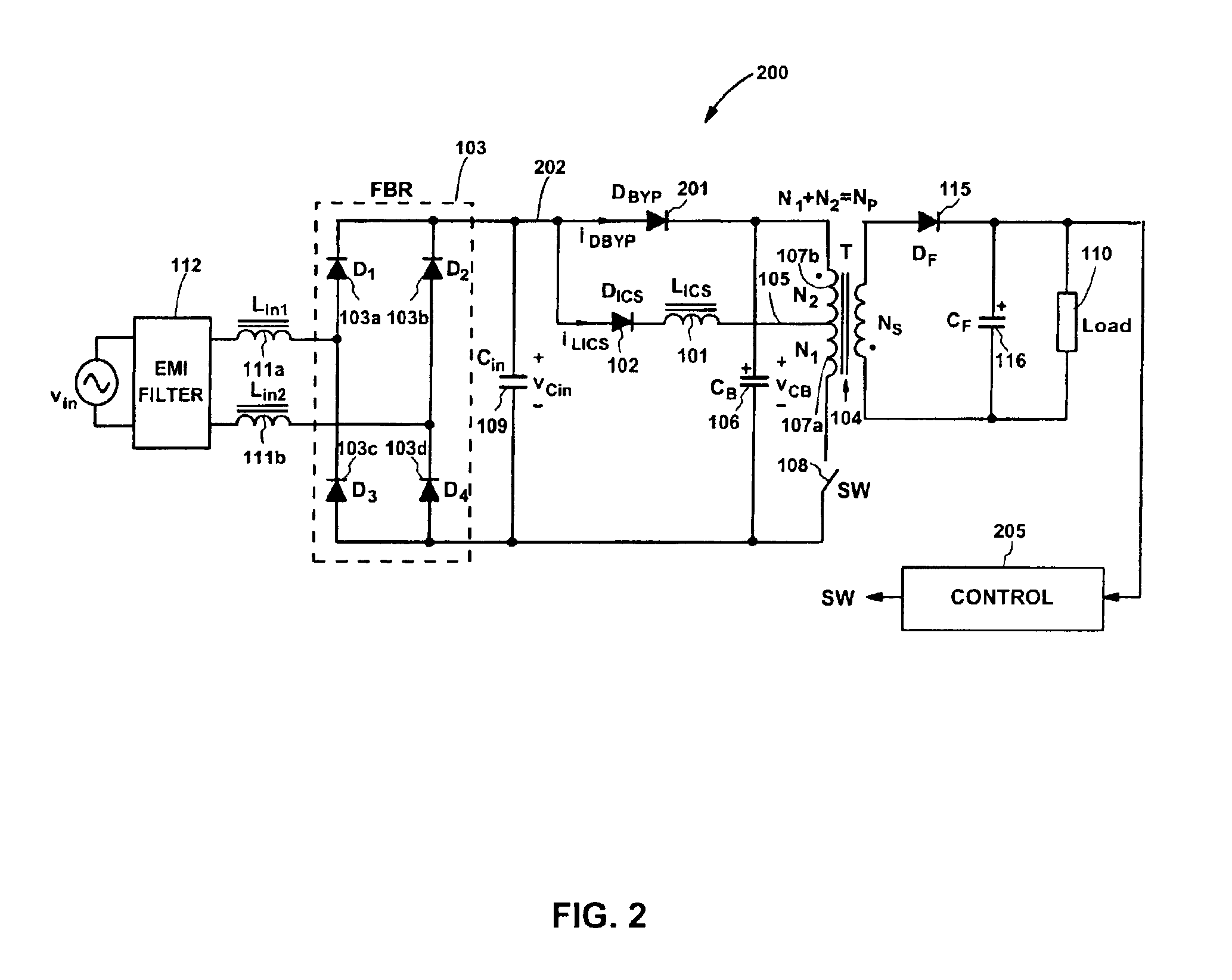
[0038]FIG. 2 is a circuit diagram of S2ICS flyback converter 200, according to one embodiment of the present invention. As shown in FIG. 2, S2ICS flyback converter 200 is substantially the same as S2ICS flyback converter 100 of FIG. 1, except that bypass diode 201 (DBYP) is connected between the positive terminal of full-bridge rectifier (FBR) 103 and the positive terminal of energy-storage (bulk) capacitor 106 (CB). A control circuit 205 provides a control signal SW for periodically opening and closing switch 108, according to a switching control scheme. One such scheme, for example, opens and closes switch 108 at a variable frequency such that transformer 104 operates at the boundary between discontinuous and continuous conduction modes. Secondary-side rectifier 115 can be implemented either with a Schottky rectifier or with a synchronous rectifier.
[0039]FIGS. 3(a), 3(b) and 3(c) illustrate the basic operation of bypass diode 201 and the effects of diode 201 on the ICS waveforms. ...
PUM
 Abstract
Description
Claims
Application Information