Image display device

a display device and image technology, applied in the direction of discharge tube luminescnet screen, discharge tube/lamp details, discharge tube main electrode, etc., can solve the problems of display defect, electron source often destroyed, electron source positioned on the outermost periphery of the display region,

Inactive Publication Date: 2008-04-08
PANASONIC LIQUID CRYSTAL DISPLAY CO LTD +1
View PDF2 Cites 1 Cited by
  • Summary
  • Abstract
  • Description
  • Claims
  • Application Information

AI Technical Summary

Benefits of technology

[0015]The electric charge injected during the manufacturing process is absorbed by the dummy potential fixing electrode on the outermost periphery of the display region, and the electron sources for display operation are protected from destruction.

Problems solved by technology

In the image display device using this type of thin-film type electron sources, electron sources are often destroyed due to unexpected electric charge or discharge during the manufacturing process or the display operation.
In particular, the electron sources positioned on the outermost periphery of the display region are often destroyed.
When electron sources are destroyed, display defect occurs, and all electron sources connected to data line may fall into display failure.

Method used


Image

  • Image display device
  • Image display device
  • Image display device

Examples


embodiment 1

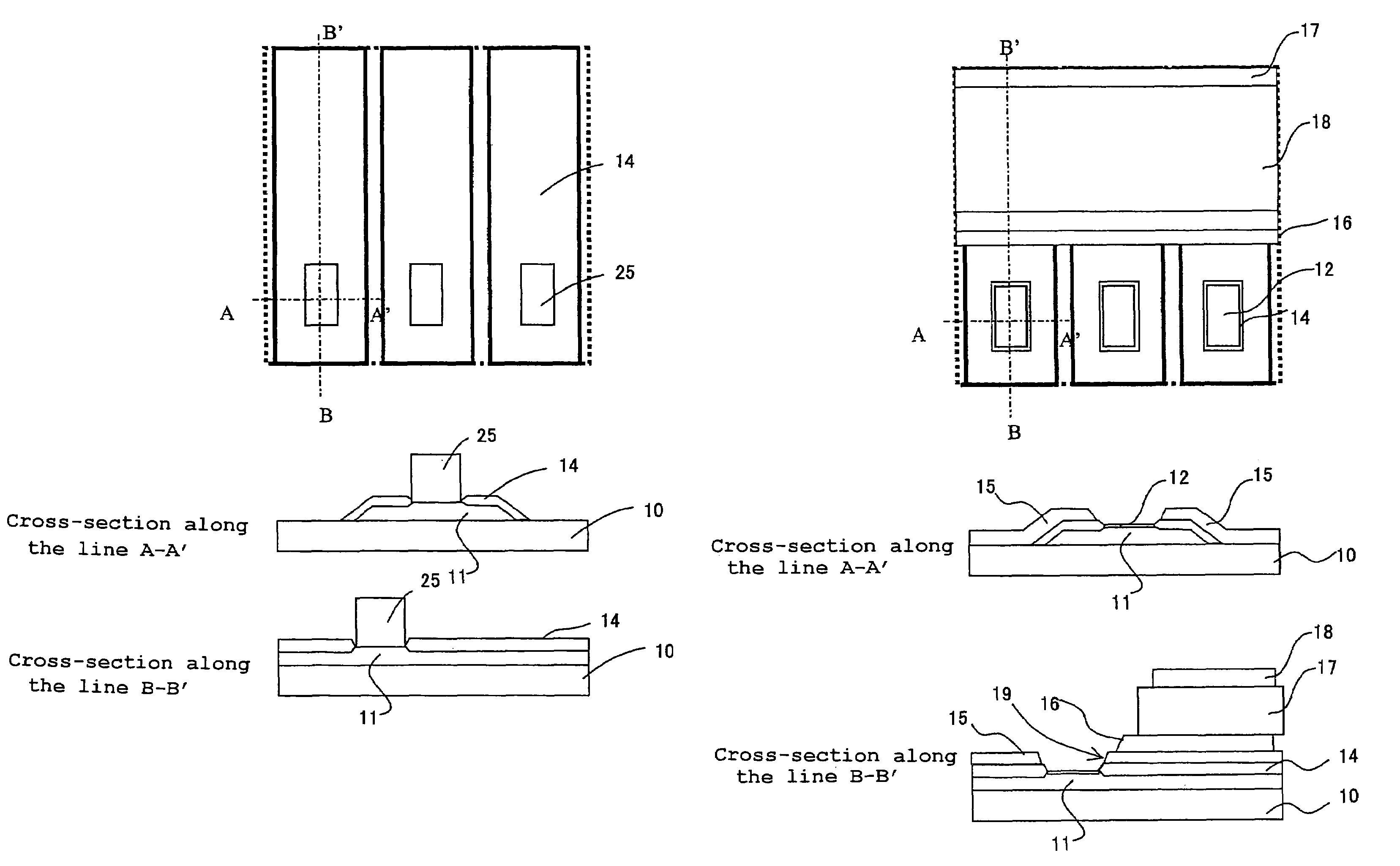
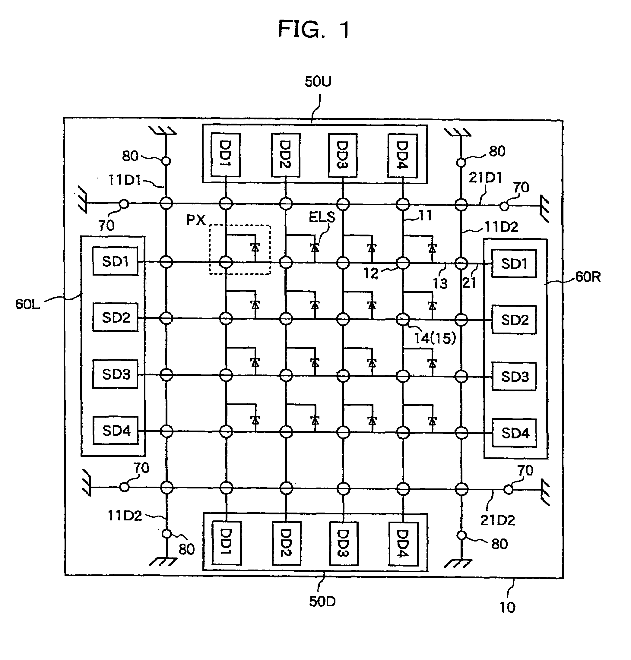
[0029]FIG. 1 is a schematical plan view of a cathode substrate to explain Embodiment 1 of an image display device according to the present invention. A bottom electrode 11, serving as data line, and a top electrode 13, to which electric current is supplied via a scan line (scan line bus) 21 in FIG. 1, are arranged (normally crossing perpendicularly to each other) on inner surface of a cathode substrate 10 preferably made of glass and positioned at an intersection via a field insulator 14 and an interlayer insulator 15. At the intersections, pixels PX comprising electron sources ELS are arranged in form of matrix.

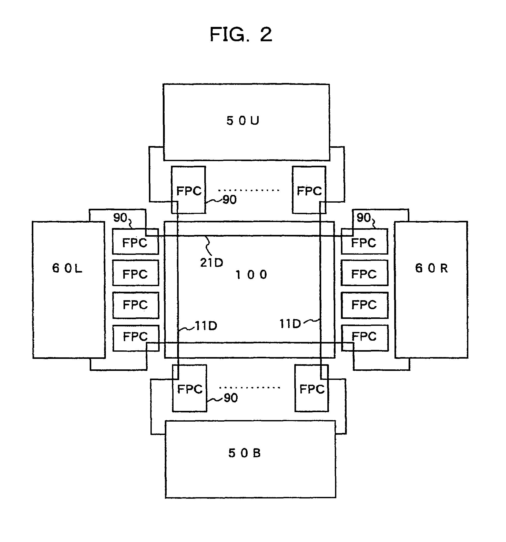
[0030]The bottom electrode 11, serving as data line, is directly provided above and below the cathode substrate 10 or it is driven by data line driving circuits 50U and 50D connected with a flexible printed board. The data line driving circuits 50U and 50D comprise data line driving circuit chips DD1, DD2, DD3, DD4, . . . corresponding respectively to the bottom electrode 11...


PUM


Abstract

The present invention provides an image display device free of display defects and with high reliability to prevent destruction of electron sources due to injection of electric charge.On the outermost periphery of a display region, there are provided a bottom electrode 11 serving as data line, a scan line bus 21 serving as scan line, and dummy potential fixing electrodes 11D1, 11D2, 21D1 and 21D2 not contributing to image display, and these are connected with electrodes 70 and 80 with low impedance and constant potential.

Description

CLAIM OF PRIORITY[0001]The present application claims priority from Japanese application JP 2005-069630 filed on Mar. 11, 2005, the content of which is hereby incorporated by reference into this application.BACKGROUND OF THE INVENTION[0002]The present invention relates to an image display device. In particular, the invention relates to an image display device, which is also called a flat panel display of emissive type using thin-film type electron source array.[0003]A type of image display device (field emission display; FED) has been developed, which uses emission type electron sources in micro-size and of integratable type, also called thin-film type electron sources. In this type of image display device, electron source is divided to emission type electron source and hot electron type electron source, etc. Those belonging to the former group include: Spindt type electron source, surface conduction type electron source, carbon nano-tube type electron source. Those belong to the la...

Claims


Application Information

Patent Timeline
Patent Type & Authority Patents(United States)
IPC IPC(8): H01J1/62
CPCH01J29/003H01J29/021H01J29/46H01J31/127H01J2329/00
Inventor SAGAWA, MASAKAZUWATANABE, TOSHIMITSUMIKAMI, YOSHIROKUSUNOKI, TOSHIAKISUZUKI, MUTSUMI
Owner PANASONIC LIQUID CRYSTAL DISPLAY CO LTD
Why Eureka
Try Eureka