Electroluminescent display
a technology of electroluminescent display and display screen, applied in the direction of identification means, instruments, static indicating devices, etc., can solve the problems of distorted waveform of power supply voltage and non-uniform brightness
- Summary
- Abstract
- Description
- Claims
- Application Information
AI Technical Summary
Benefits of technology
Problems solved by technology
Method used
Image

Examples
first embodiment
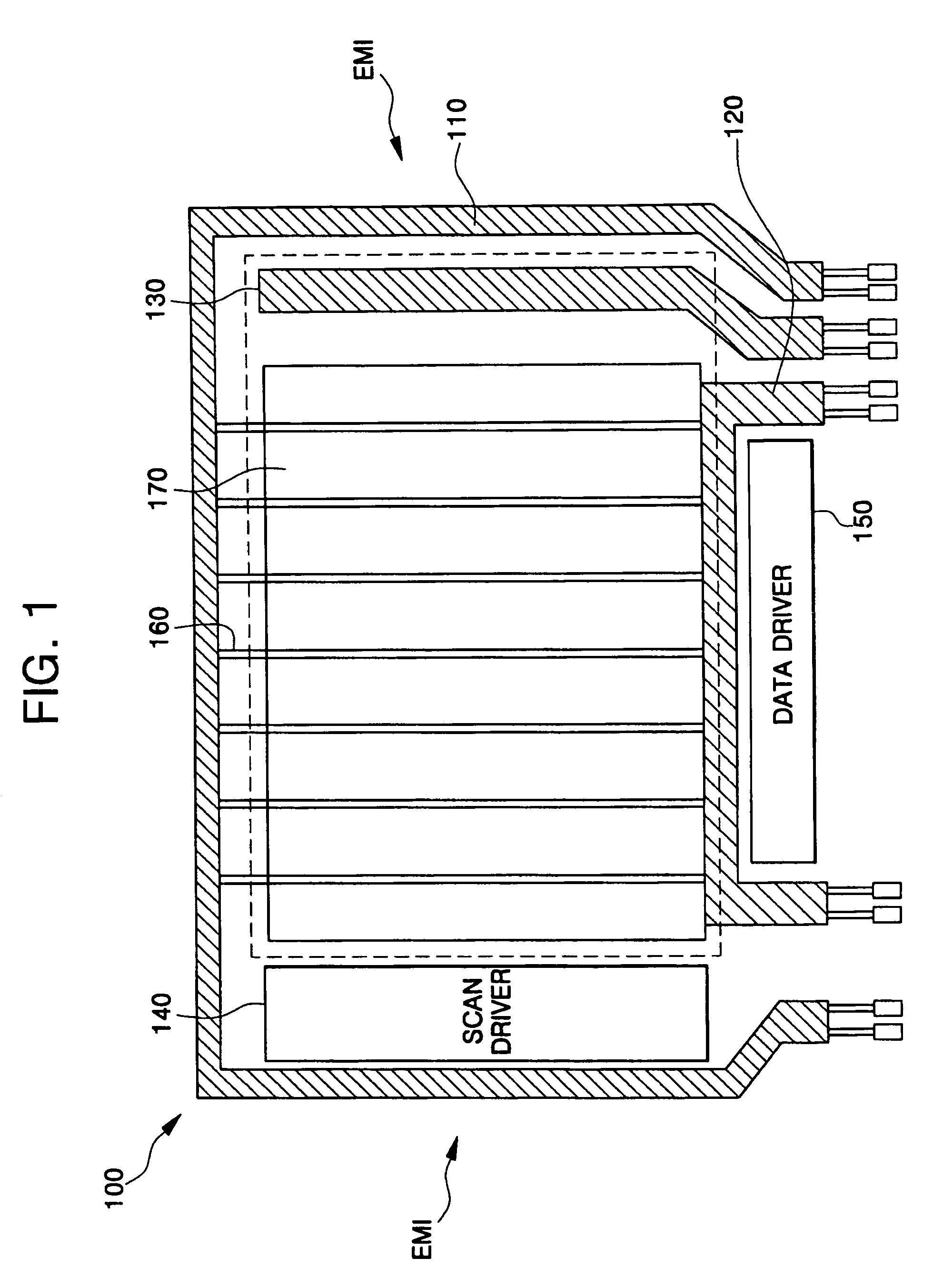
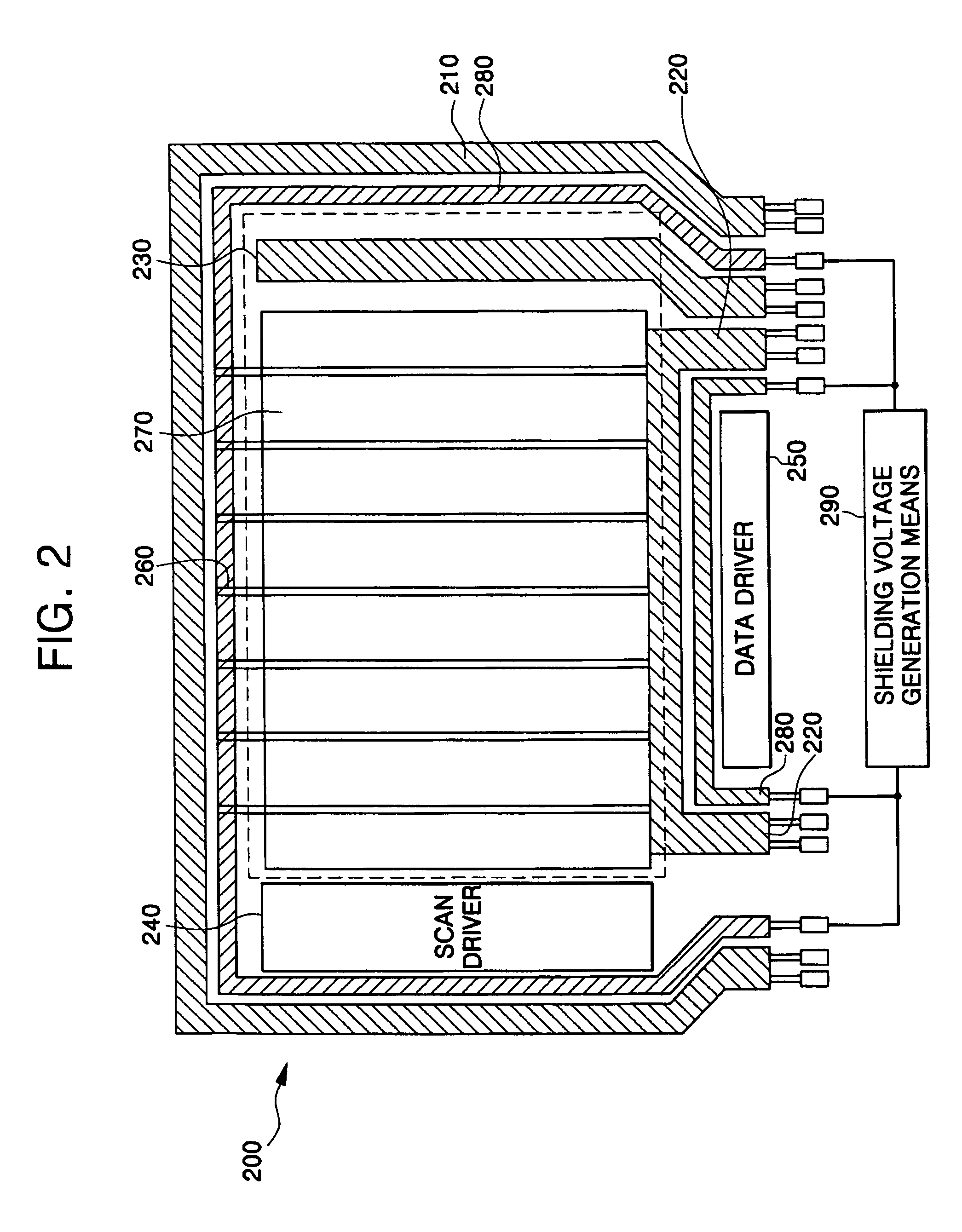
[0036]FIG. 2 is a plan view of an electroluminescent display in accordance with the present invention.
[0037]An electroluminescent display 200 includes a first upper power supply line 210, a first lower power supply voltage line 220, a second power supply voltage line 230, a scan driver 240, a data driver 250, a first active power supply voltage line 260, a pixel region 270, a metal line 280, and a shielding voltage generator 290.
[0038]As shown in FIG. 2, the electroluminescent display 200 according to an embodiment of the present invention includes the scan driver 240, the data driver 250, the pixel region 270 emitting light in response to a selection signal and a data signal respectively supplied by the scan driver 240 and the data driver 250, the first upper and lower power supply voltage lines 210 and 220 delivering first power supply voltages, the first active power supply voltage line 260 supplying the power supply voltages from the first power supply voltage lines 210 and 220 ...
second embodiment
[0043]FIG. 3 is a plan view of an electroluminescent display in accordance with the present invention.
[0044]As shown in FIG. 3, another embodiment of the present invention has ground terminals 291, each of which being connected to the metal line 280. Accordingly, the electromagnetic waves supplied to the first power supply voltage lines 210 and 220 are attracted by the metal line 280 to be grounded so that the power supply voltages are shielded from the electromagnetic waves.
third embodiment
[0045]FIG. 4 is a plan view of an electroluminescent display in accordance with the present invention.
[0046]As described above, the metal line 280 is arranged in the first upper power supply voltage line 210 as in the first embodiment. However, in the third embodiment, the metal line 280 can also be arranged outside the first upper power supply voltage line 210.
[0047]That is, the metal line 280 is arranged outside the first upper power supply voltage line 210 so as to be spaced apart or insulated from the first upper power supply voltage line 210 by a constant interval or by an insulator (not shown) respectively, so that the electromagnetic waves from an external source can be shielded.
PUM
 Abstract
Description
Claims
Application Information
 - R&D
- Intellectual Property
- Life Sciences
- Materials
- Tech Scout
- Unparalleled Data Quality
- Higher Quality Content
- 60% Fewer Hallucinations
Browse by: Latest US Patents, China's latest patents, Technical Efficacy Thesaurus, Application Domain, Technology Topic, Popular Technical Reports.
© 2025 PatSnap. All rights reserved.Legal|Privacy policy|Modern Slavery Act Transparency Statement|Sitemap|About US| Contact US: help@patsnap.com