Low power memory controller with leaded double data rate DRAM package on a two layer printed circuit board

a memory controller and printed circuit board technology, applied in the field of low power memory controllers placed on two-layer printed circuit boards, can solve the problems of increasing the overall complexity of the packaged integrated circuit, limiting the selection of available packing techniques, and requiring additional cost savings, so as to achieve substantial cost savings, cost savings, and additional cost savings

a memory controller and printed circuit board technology, applied in the field of low power memory controllers placed on two-layer printed circuit boards, can solve the problems of increasing the overall complexity of the packaged integrated circuit, limiting the selection of available packing techniques, and requiring additional cost savings, so as to achieve substantial cost savings, cost savings, and additional cost savings

US7657774B1Inactive Publication Date: 2010-02-02BROADCOM INT PTE LTD

Image

  • Low power memory controller with leaded double data rate DRAM package on a two layer printed circuit board
  • Low power memory controller with leaded double data rate DRAM package on a two layer printed circuit board
  • Low power memory controller with leaded double data rate DRAM package on a two layer printed circuit board

Examples


Embodiment Construction

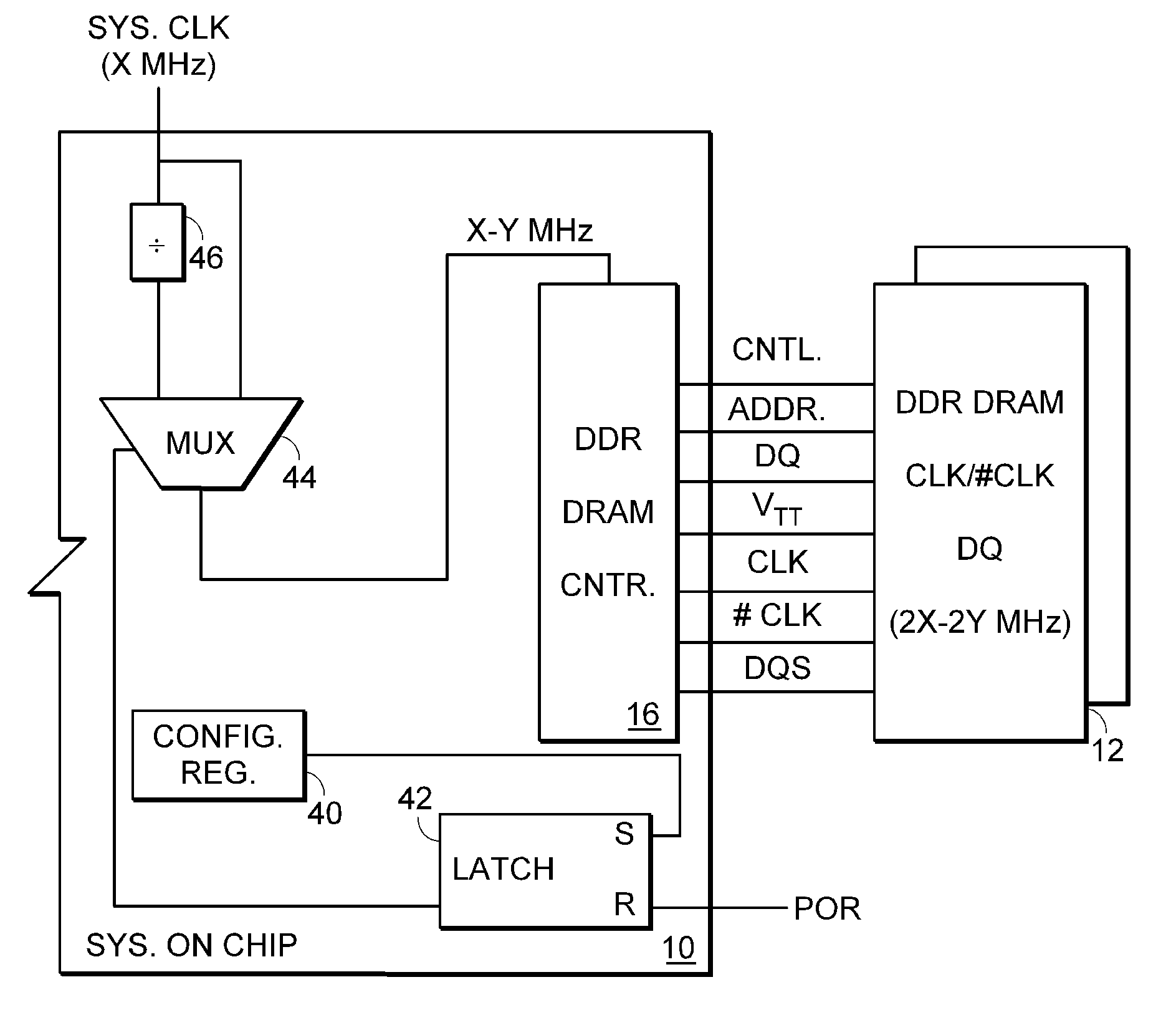
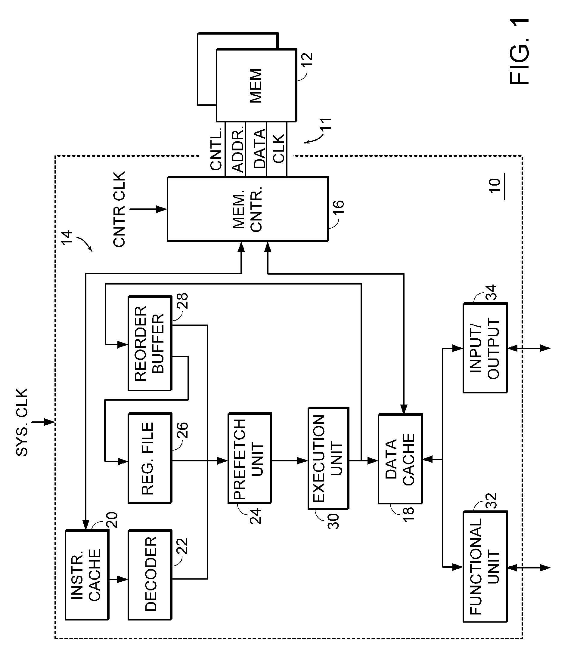
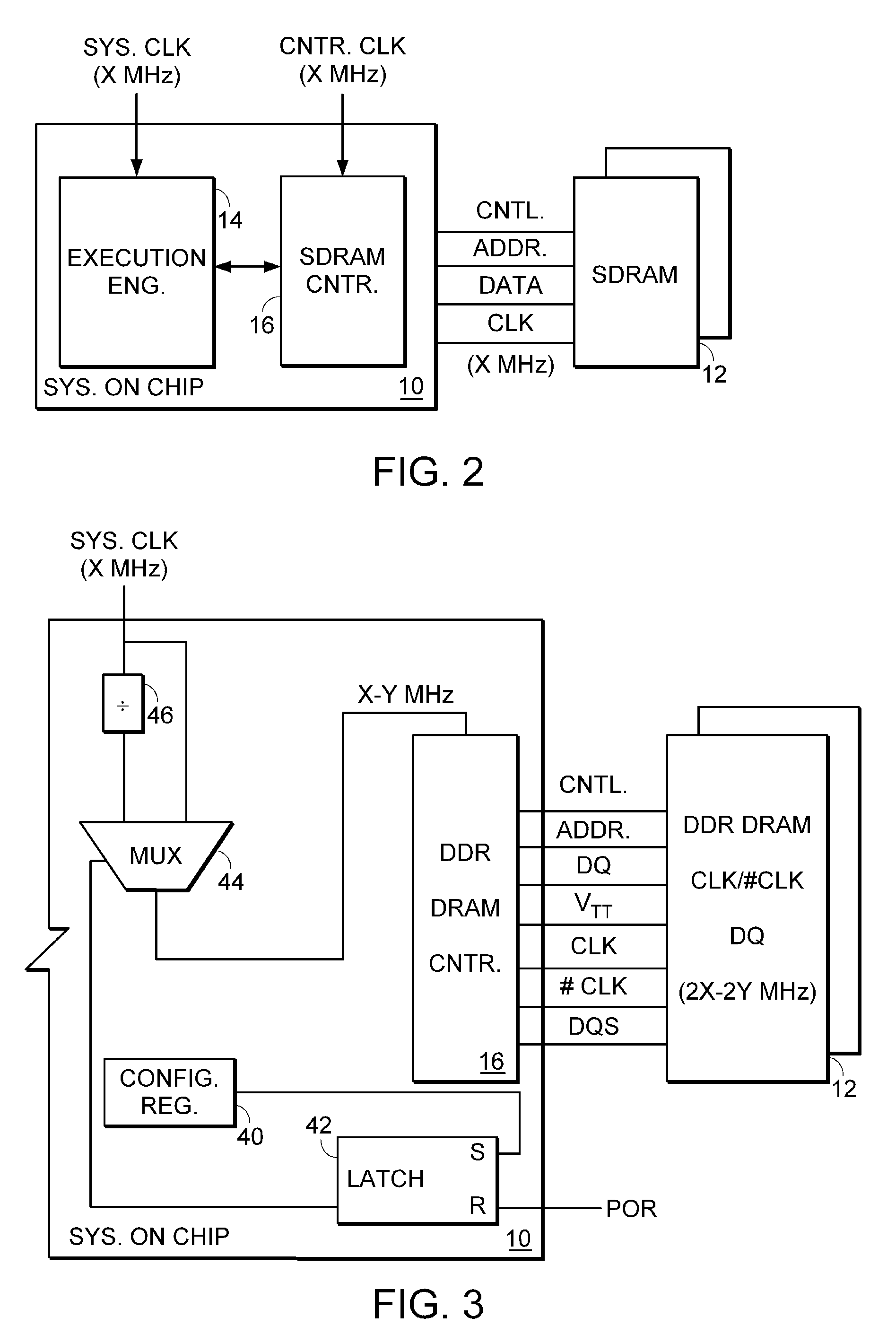
[0037]Turning now to the drawings, FIG. 1 illustrates a memory module having a series of semiconductor memory devices 12 connected to a memory controller 16. A memory bus 11 is used to convey information between the memory devices 12 and a memory controller 16. Each semiconductor memory device 12 is preferably an asynchronous DDR dynamic random access memory (DRAM) device. Also, each memory device 12 includes an array of storage cells formed on separate chips of a semiconductor wafer, wherein the separate chips are removed and placed on a paddle of a lead frame. The paddle, chip, and a portion of the lead frame are preferably sealed inside a package. The package includes leads that extend from an outer surface of the package. Thereafter, the leads can be forwarded into holes or affixed to conductors on the surface of a PCB. There are various types of packages, some of which are through-hole dual in-line packages (DIP), j-leaded chip carriers, leadless chip carriers, etc., all of whi...


PUM


Abstract

An integrated circuit is provided that includes an execution engine and a memory controller. The execution engine is clocked at a first rate and the memory controller is clocked at a second rate that is less than the first rate. Pins on the integrated circuit can transfer data to and from the integrated circuit on both the rising and falling edges of a second clock transitioning at the second clock rate. The integrated circuit is preferably packaged using a lead frame and wire bonds extending from pads on the integrated circuit to corresponding leads. The leads are secured to trace conductors on a surface of a printed circuit board. The board contains no more than two conductive layers separated by a dielectric layer. Thus, an overall electronic system is formed having a board with no more than two conductive layers, an execution engine that receives a first clock signal, a memory controller which receives a second clock signal, and a memory device that sends data to and from the memory controller at twice the rate of the second clock signal. Using a throttled second clock signal allows for less expensive packaging and mounting of packaged integrated circuits on a less expensive PCB, while still maintaining use of a DDR DRAM transfer mechanism.

Description

CONTINUING DATA[0001]The present application is a continuation from prior U.S. patent application Ser. No. 10 / 728,492 filed Dec. 5, 2003 which is incorporated herein by reference.BACKGROUND OF THE INVENTION[0002]1. Field of Invention[0003]This invention relates to semiconductor memory and, more particularly, to a low power memory controller placed on a two-layer printed circuit board (PCB) with a double data rate (DDR) DRAM, both of which are packaged with leads extending outward from the package and secured to pads on the PCB for a lower cost semiconductor memory system.[0004]2. Description of Related Art[0005]The following descriptions and examples are not admitted to be prior art by virtue of their inclusion within this section.[0006]There are numerous types of memories available in the marketplace. For example, large volumes of data can be stored in magnetic memory, such as a hard disk drive. Lesser quantities of data can be stored in memory arranged upon an integrated circuit, ...

Claims


Application Information

Patent Timeline
02 Feb 2010
Publication
US7657774B1
IPC
G06F1/00; G06F1/04; G06F12/00; H05K1/00
CPC
G06F1/3203; G06F1/324; G06F1/3275; Y02B60/1228; Y02B60/1217; Y02D10/00
Inventors
HUNG, ERIC; DESAI, GEETA K.