
Photosensitive organic semiconductor compositions
a semiconductor and composition technology, applied in semiconductor devices, solid-state devices, electrical devices, etc., can solve the problems of fragile sublimed films, prone to damage, and high production costs of prior art formulations of organic semi-conducting materials
Patent Information
- Authority / Receiving Office
- US · United States
- Patent Type
- Applications(United States)
- Current Assignee / Owner
- Publication Date
- 2006-08-17
- Estimated Expiration
- Not applicable · inactive patent
Smart Images
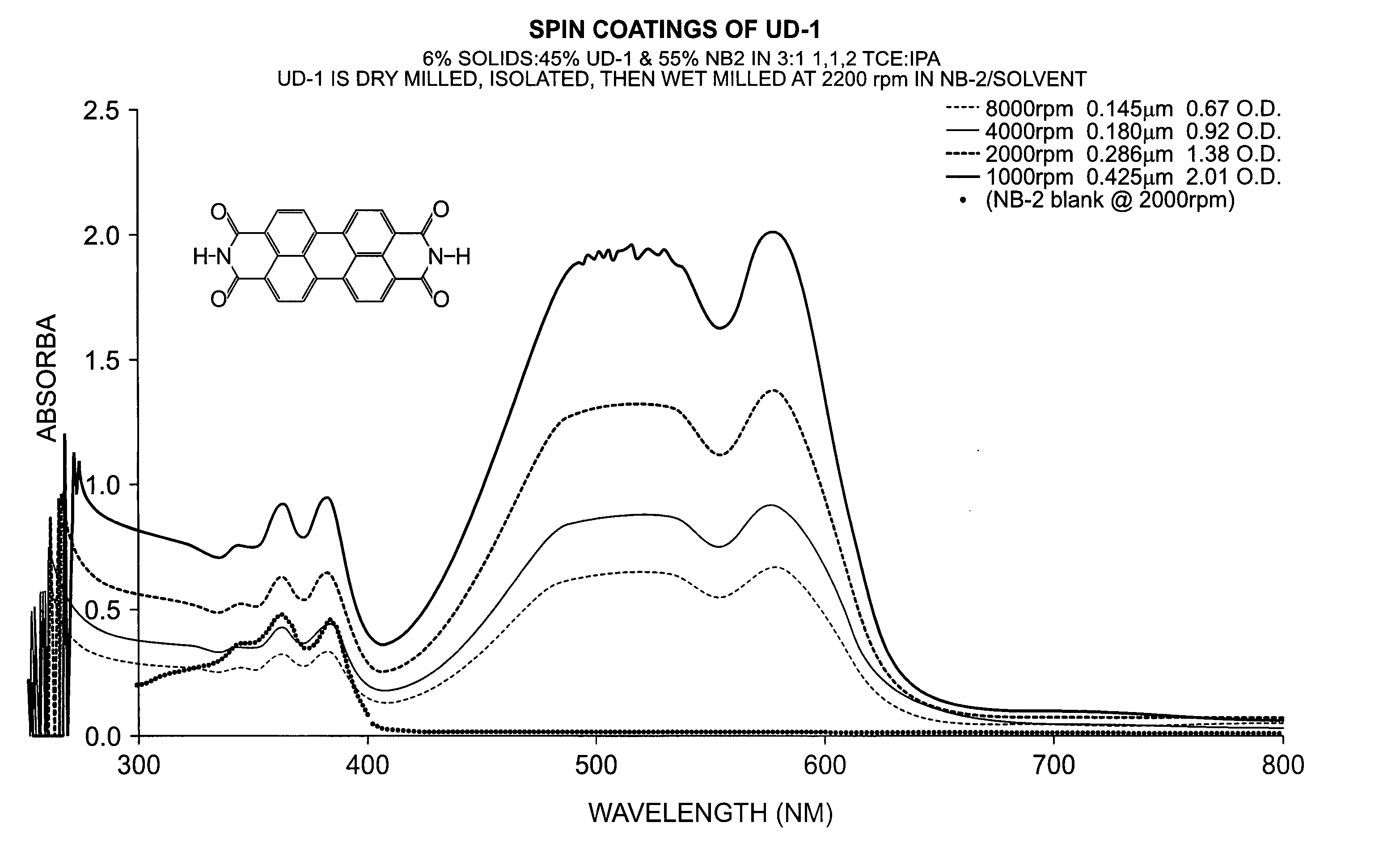
Figure 1 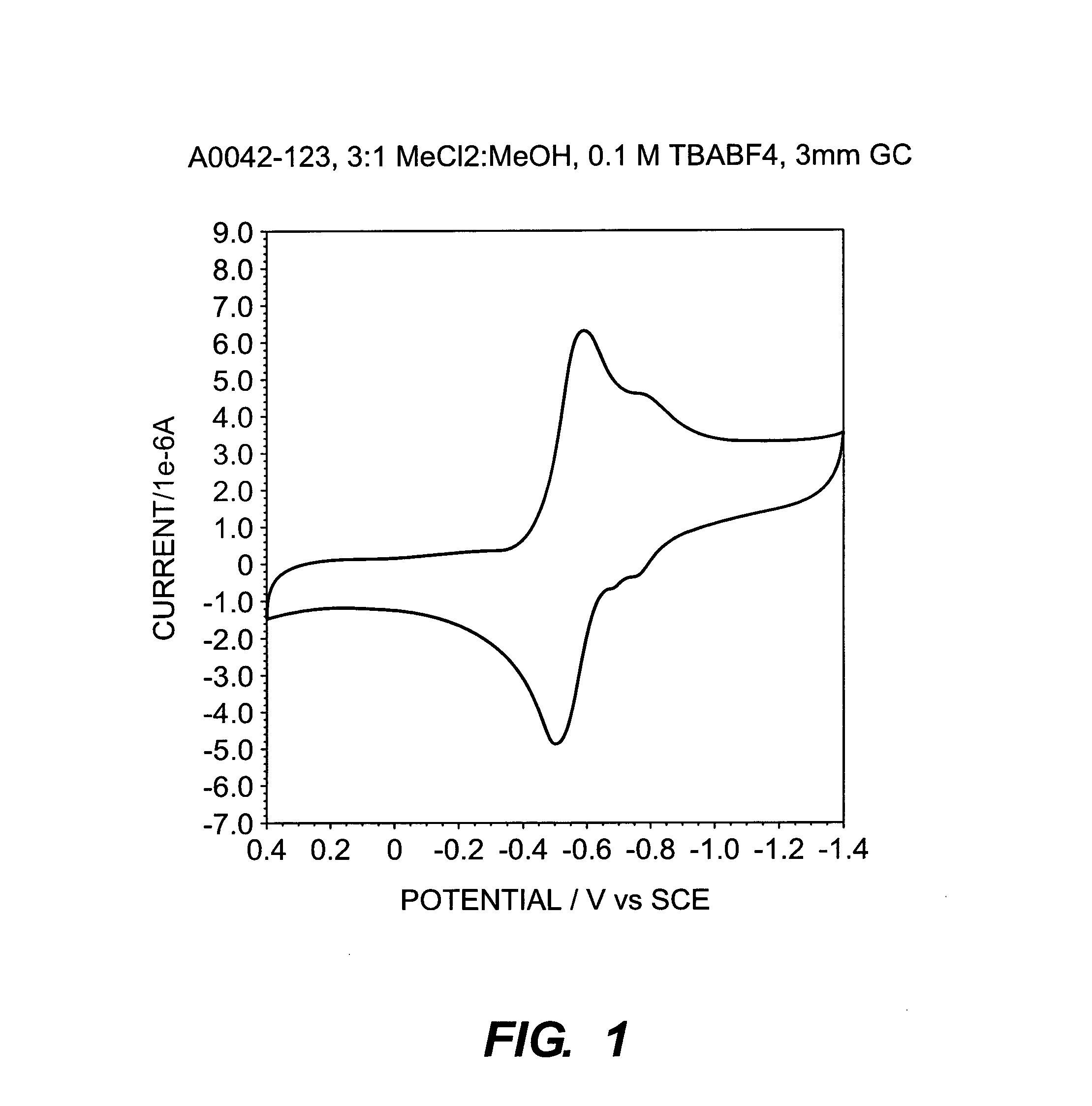
Figure 2 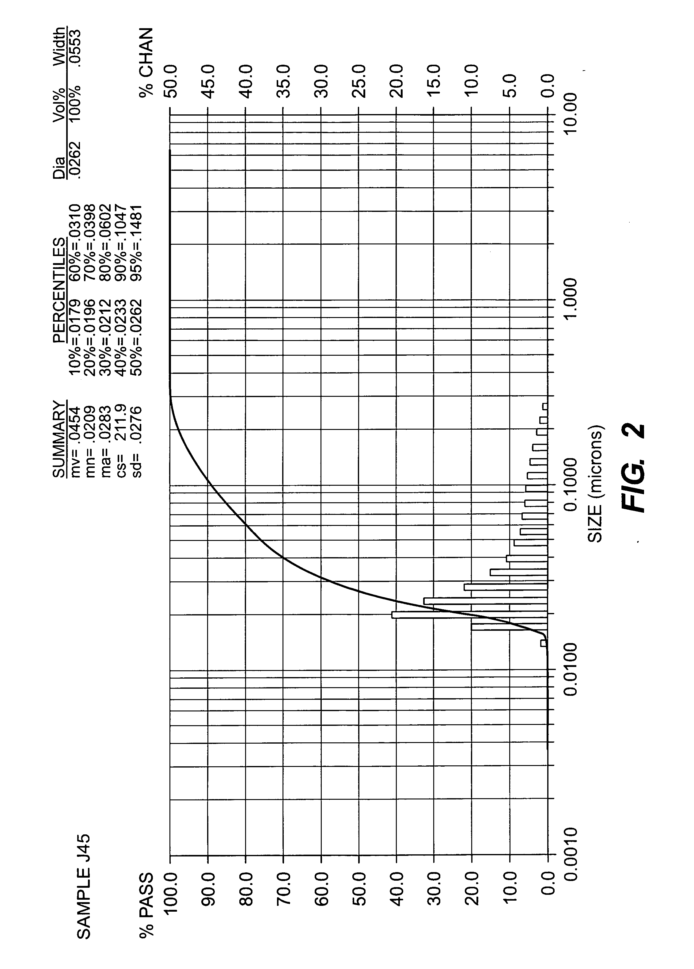
Figure 3
Abstract
Description
FIELD OF THE INVENTION
[0001] The present invention relates to photosensitive organic semiconductor compositions. BACKGROUND OF THE INVENTION
[0002] There is widespread interest in developing photosensitive organic semiconductor compositions for use in various optoelectronic devices, including photovoltaics (solar cells) and visible light photodetectors. Such optoelectronic devices typically incorporate a p / n heterojunction formed at the interface between p-type and n-type semiconducting layers. For organic materials the designation “n-type” indicates the material to exhibit electron accepting character, and as such is considered capable of transporting electrons. The measure of electron accepting character is usually provided either by the electron affinity or electrochemical reduction potential of the organic material. A “p-type” organic material, on the other hand, is considered to have electron donating character and as such is considered to be “hole transporting”. The measure o...
Examples
example 1
[0046] An n-type (electron acceptor) semiconductor composition of a stable dispersion of nanoparticle semiconductor pigment in a solvent solution of an electronically conducting polymer was prepared using the semiconductor pigment material 3,4,9,10-perylenetetracarboxylic dianhydride compound denoted as UD-1 (structure below). The pigment is a perylene diimide useful in the preparation of photodiodes for photovoltaics and other optoelectronic applications. The pigment was milled to a small particle size and dispersed in the n-type electronically conducting polymer derived from 1,4,5,8-naphthalenetetracarboxylic dianhydride. The electrochemical reduction potential of the naphthimide containing polymer NB-2 is similar, that is within 0.2 V, of the reduction potential of a perylene diimide material.
[0047] The conducting polymer NB-2 is comprised of the following component parts: 12.5% DDA, 15% NX62, 2.5% AB, 5% EO2EA, 5% NB3, 30% NX3, and 30% NB10.
[0048] The electronically conducti...
example 2
[0054] A ball mill (1 gal glass) was charged with 9000 g of ⅛ inch chrome steel beads and 75.0 g of titanium, oxo(29H,31H-phthalocyaninato(2-)-.kappa.N29,.kappa.N30,.kappa.N31,.kappa.N32)-, (SP-5-12)-[C32H16N8 O Ti]“TiOPc” containing 1.3 wt % chlorine impurity. The mixture was sheared by milling at about 110 rpm for 7 days at room temperature (about 23° C.). A sample of the resulting pigment was extracted from the beads with water and then dried over night under vacuum at room temperature. 5970 g of the milled pigment with beads was transferred to a 250 ml glass jar, 1305 g of dichloromethane (DCM) was added and the mixture was milled another 24 hours at 117 rpm at room temperature. After this second milling, the pigment / DCM slurry was decanted into a clean 1 gal glass jar. The beads were rinsed 3 times with fresh DCM, and the resulting pigment / DCM was also added to the 1 gal glass jar. The pigment was filtered through a 350 ml medium glass frit under water stream vacuum. The result...
example 3
[0060] A photovoltaic cell is prepared by first spin coating a 100 nm thick layer of the p-type TiOpc semiconductor crystal pigment / conducting polymer dispersion described in Example 1 onto a transparent flexible (plastic) support bearing a thin film of indium tin oxide transparent conductor (8 ohm / sq). On a second piece of transparent flexible (plastic) support bearing a thin film of indium tin oxide transparent conductor is coated a 100 nm thick layer of the n-type UD-1 semiconductor crystal pigment / conducting polymer dispersion described in example 3. Each of the coated layers is gently heated under vacuum to remove residual solvent. The two plastic supports thusly coated and dried are pressed together via lamination using a heated roller assembly, with the two plastic supports remaining slightly offset during lamination to allow for electrical connections. The temperature of the rollers is adjusted to a few degrees above the glass transition temperature of the polymers. Electric...