
Circuit module having interleaved groups of circuit chips

A kind of circuit chip, circuit module technology

Inactive Publication Date: 2008-04-16
INFINEON TECH AG
View PDF4 Cites 0 Cited by
  • Summary
  • Abstract
  • Description
  • Claims
  • Application Information

AI Technical Summary

Problems solved by technology

The arrangement of the memory chips as explained above, in which the memory chips belonging to the same memory group are arranged in the same layer, so heat dissipation is difficult
So, the temperature of the memory module can reach 80 to 90°C, especially, if the bottom chipset drives, the heat convection to the surrounding air is quite bad, and this may cause damage to the memory chips, and thus the memory module's damage

Method used


Image

  • Circuit module having interleaved groups of circuit chips

Examples


Embodiment Construction

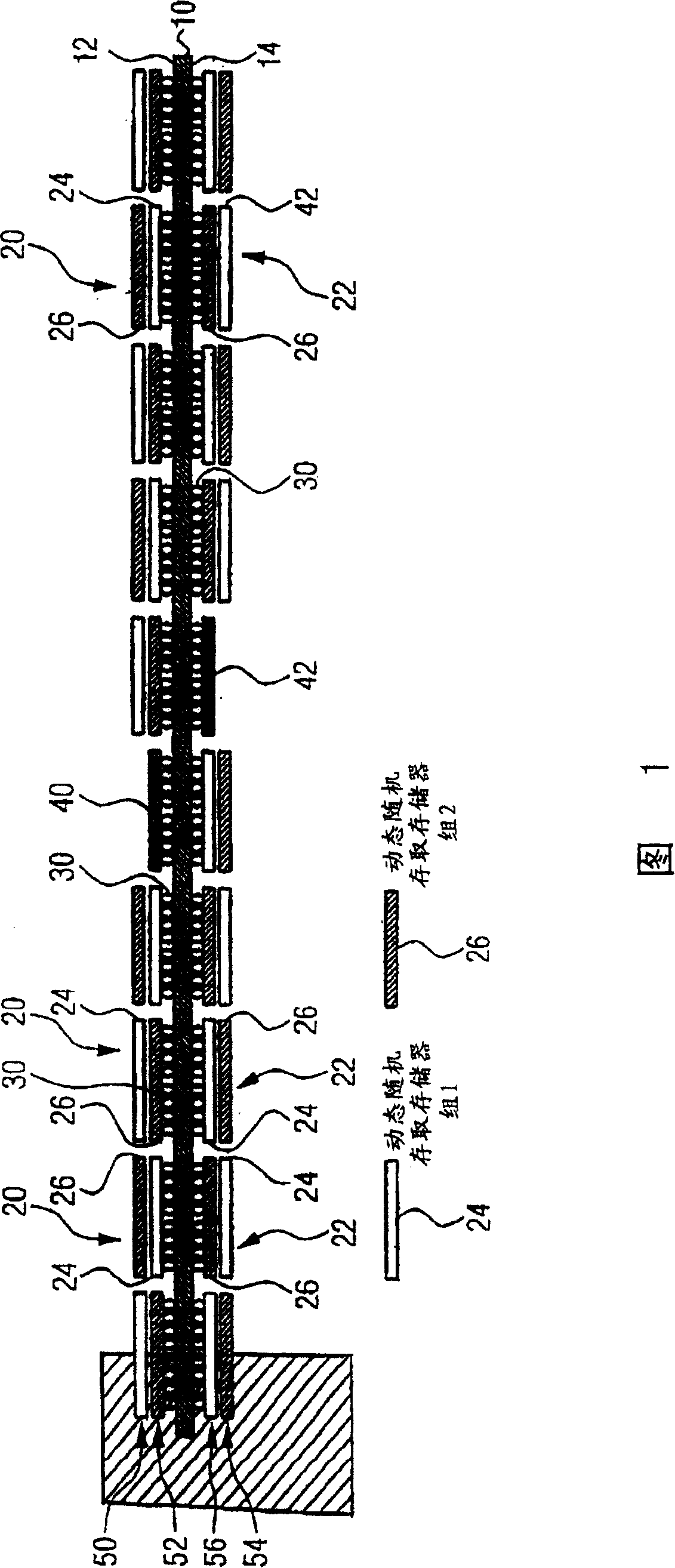
[0019] FIG. 1 shows a schematic diagram of a memory module in the form of a server dedicated DIMM (registered DIMM) to represent a circuit module according to the present invention. The memory module comprises a module board 10 having a first major surface 12, and a second major surface 14 opposite the first major surface, on which a stack 20 of memory chips is formed, The stack 22 is formed on the second major surface 14 . To illustrate this embodiment in more detail, as shown in FIG. 1 , nine stacks 20 are formed on the first major surface 12 and nine stacks 22 are formed on the second major surface 14 .

[0020] Each of the stacks 20 and 22 includes two circuit chips 24 and 26, and the circuit chip 24 belongs to a first DRAM group, DRAM group 1, and conversely, the memory chip 26 indicated by hatching in FIG. Belongs to a second DRAM group, DRAM group 2.

[0021] The individual stacks of memory chips can be implemented in a manner known to those familiar with such memorie...


PUM


Abstract

A circuit module has a carrier (10) and multiple stacks (20, 22) of circuit chips (24, 26) arranged on a surface (12, 14) of the carrier (10). Each stack has multiple circuit chips arranged in different layers (50, 52, 54, 56). The circuit chips are grouped in different groups, wherein the groups are not active at the same time. The circuit chips are arranged such that circuit chips belonging to the same group are arranged in different layers in adjacent stacks.

Description

technical field [0001] The present invention relates to a circuit module, and more particularly, to a circuit module contained in a carrier and a circuit chip set disposed on the carrier, wherein the circuit chips are classified into different groups driven at different times. Background technique [0002] The traditional structure of the memory module, DIMMs (dual in-line memory module, Dual In-LineMemory Module), for example, includes a module board (module board) and, for example, the memory chip, DRAM configured on the module board groups of chips. In a high-density memory module, the memory chips are stacked on the module board, wherein each stack includes a plurality of memory chips stacked on top of each other, typically, each stack includes two chips, one configured in a first layer of the stack, and one is disposed in a second layer of the stack. [0003] And in such conventional memory modules, the memory chips are classified into two memory chip groups (banks), ...

Claims


Application Information

Patent Timeline
Patent Type & Authority Patents(China)
IPC IPC(8): G11C5/02H01L25/065H01L27/108H05K1/18
CPCH01L2924/0002H01L27/10897H05K1/181H05K2201/10522H01L25/0652H05K2201/10515H05K2201/10159Y02P70/50H10B12/50H01L2924/00
Inventor S·切努帕蒂
Owner INFINEON TECH AG
Learn More