

Surface polishing method for protective side edge of group II-VI semiconductor material
A surface polishing and semiconductor technology, applied in the direction of surface polishing machine tools, semiconductor/solid device manufacturing, grinding/polishing equipment, etc., can solve problems such as gaps, crack defects, debris, etc.
- Summary
- Abstract
- Description
- Claims
- Application Information
AI Technical Summary
Problems solved by technology
Method used
Image

Examples
Embodiment Construction
[0018] Take the CdZnTe wafer as an example below for a detailed introduction:
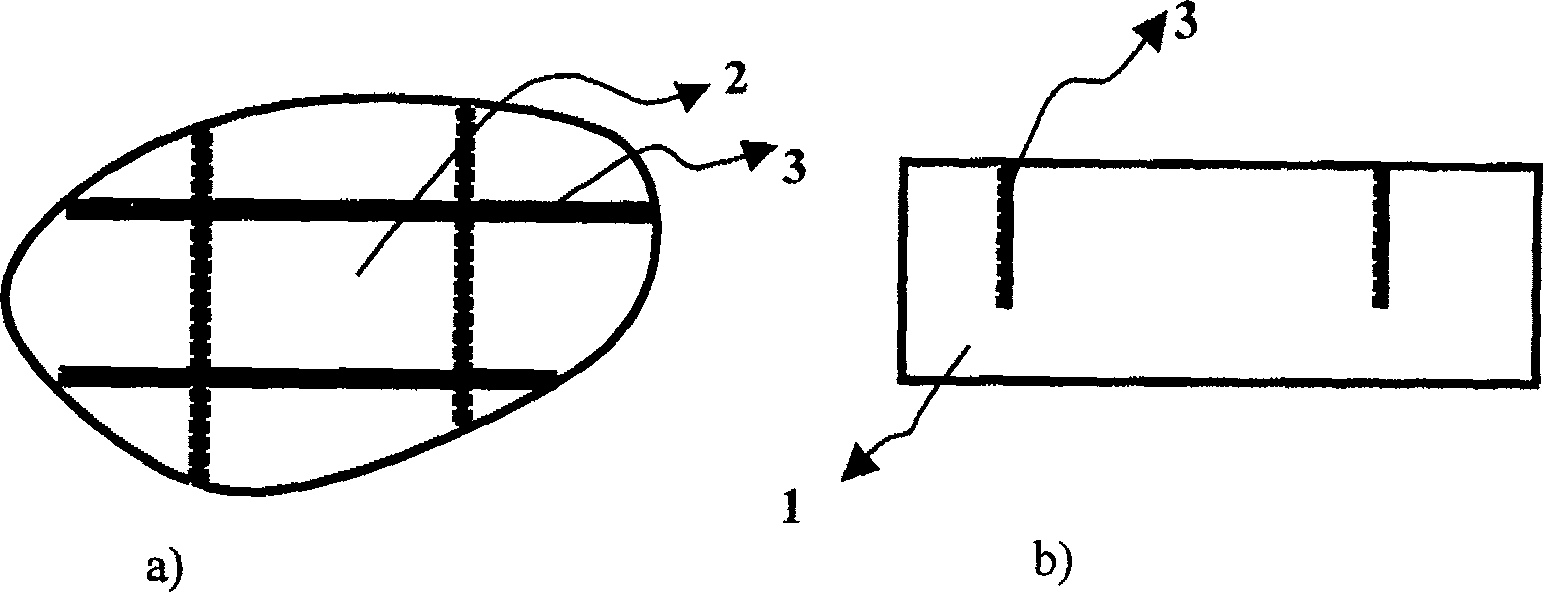
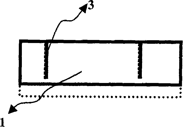
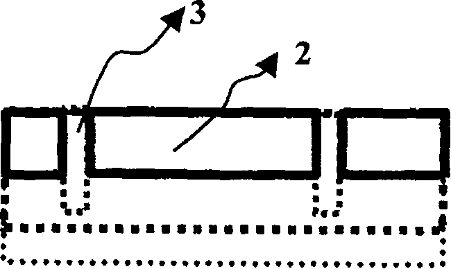
[0019] As shown in the attached figure, the thickness of the original chip 1 is 1100 microns, and the thickness of the molded wafer 2 is required to be 550 microns. First, use a dicing machine to draw the area required for the molded wafer on the surface of the original film, such as 20 mm X 30 mm, and cut the slit 3 The depth is about 600 microns, and then put wax on the surface of the original film with slits and heat it to 70 ° C. After the wax melts and sticks to the flat glass substrate, the surface of the original film is treated with a 3 micron alumina suspension. Coarse mechanical grinding, when grinding to a thickness of 608-610 microns, then mechanical chemical polishing until the required thickness of 550 microns can be obtained to obtain a CdZnTe molded wafer with no damage to the side edge. Finally, after heating to soften the wax, take out the molded wafer part in the central area, an...
PUM
 Abstract
Description
Claims
Application Information