Physical address conversion device and conversion method

A physical address and conversion device technology, which is applied to secure communication devices and key distribution, to achieve the effect of simple implementation and flexible conversion

Inactive Publication Date: 2008-12-03
HUAWEI TECH CO LTD
View PDF2 Cites 0 Cited by
  • Summary
  • Abstract
  • Description
  • Claims
  • Application Information

AI Technical Summary

Problems solved by technology

[0016] The problem solved by the present invention is to avoid developing and designing multiple physical layer single boards due to physical address mismatch when the MAC layer chip or other MAC layer chips access the physical layer chip through the media independent interface

Method used


Image

  • Physical address conversion device and conversion method
  • Physical address conversion device and conversion method
  • Physical address conversion device and conversion method

Examples


Embodiment Construction

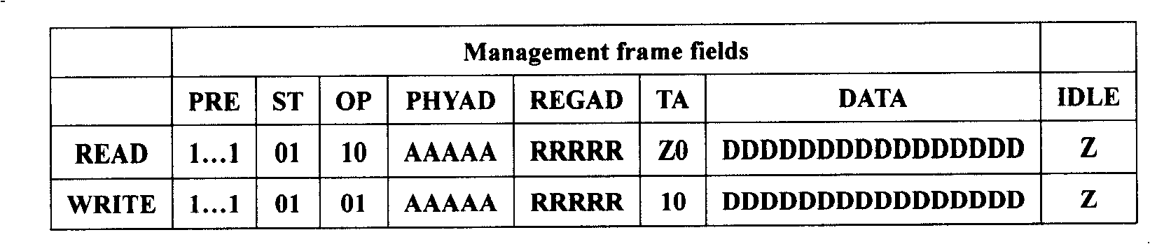
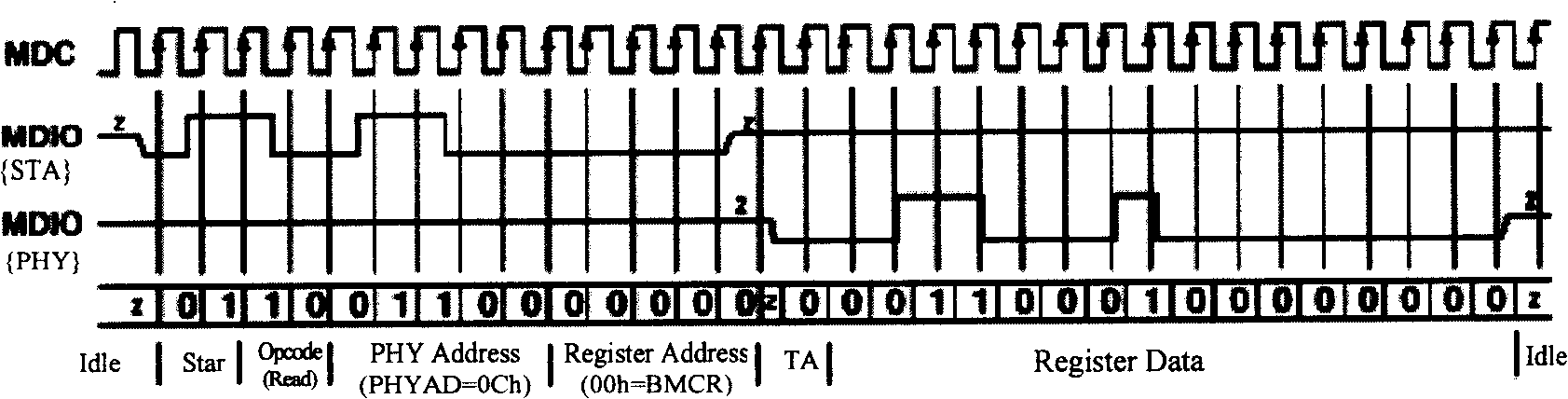
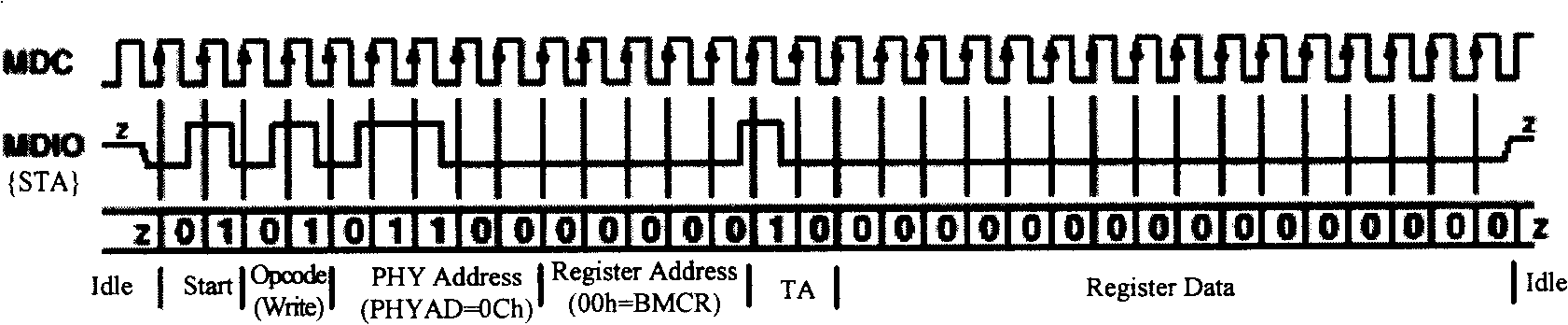
[0034] At present, because the physical addresses of many MAC layer chips are fixed, if the physical layer chips need to interface with several MAC layer chips, different hardware must be designed in the prior art to meet the requirements. The solution in the prior art solves the problem from the perspective of changing the physical address of the physical layer chip to adapt to the physical address of the MAC layer chip. And the physical address conversion device and method of the present invention solve the problem from the opposite angle: shield the MAC layer chip physical address, by converting the physical address consistent with the physical address of the physical layer chip output, the above-mentioned thus makes no matter the physical layer chip and the MAC layer chip Any value of the physical address can be connected normally. In this way, if a physical layer chip is connected to several MAC layer chips, the development of multiple physical layer single boards can be ...


PUM


Abstract

A physical address conversion device and method includes a first interface, a second interface and a conversion module, the first interface sets up a communication connection with MAC layer chip, the second interface sets up communication connection with the physical layer chip, the conversion module intercepts and shields the physical address of MAC layer chip, outputs the preserved physical address in the chip to match with the physical layer chip. A conversion method includes: preserving the address of the physical layer chip, intercepting and shielding the address of MAC Layer chip, outputting the address of the physical layer chip to the physical layer chip to match with its address for connecting with the chips of the physical layer and MAC.

Description

technical field [0001] The invention relates to communication between a physical layer chip and a MAC layer chip, a physical address conversion device and a conversion method applied in a medium-independent interface. Background technique [0002] In the field of communication, the media access control (MAC, Media Access Control) layer chip (or other MAC layer chip) can access the registers of the physical layer chip through the management interface of the media independent interface (MII, Media Independent Interface), and through these registers To control and manage the physical layer chip. The management interface includes two signal lines: management data synchronous clock input (MDC, Management Data Clock) and bidirectional management data (MDIO, Management data input / output), as follows: [0003] MDC: The clock of the management interface is a non-periodic signal. The minimum period of the signal (actually the sum of positive level time and negative level time) is 400...

Claims


Application Information

Patent Timeline
Patent Type & Authority Patents(China)
IPC IPC(8): H04L29/02H04L9/00H04L9/08
Inventor 周敏峰马金永张玉泉张海生
Owner HUAWEI TECH CO LTD
Why Eureka
Try Eureka