Triple pole structure of plane type field emission, and preparation method

A field emission, planar technology, applied in the direction of electroluminescent light source, lighting device, light source, etc., can solve the problems of glass substrate damage, high working temperature, emitter damage, etc., to reduce short circuit, overcome positioning difficulties, improve The effect of emission stability

Inactive Publication Date: 2008-12-17
SOUTHEAST UNIV
View PDF4 Cites 0 Cited by
  • Summary
  • Abstract
  • Description
  • Claims
  • Application Information

AI Technical Summary

Problems solved by technology

Although the protective layer has a certain protective effect on the cathode, it will still cause damage to some emitters and affect the performance of the display device.
If the CVD method is used in the triode structure to directly grow the emitting material in the dielectric film hole, although the difficulty of material filling can be avoided, the glass substrate is easily damaged due to the high working temperature of CVD.

Method used


Image

  • Triple pole structure of plane type field emission, and preparation method
  • Triple pole structure of plane type field emission, and preparation method
  • Triple pole structure of plane type field emission, and preparation method

Examples


Embodiment Construction

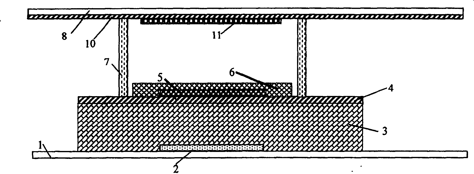
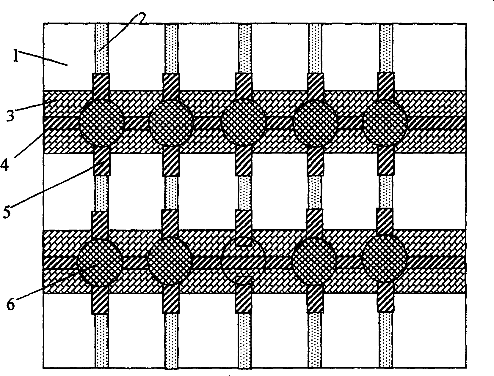
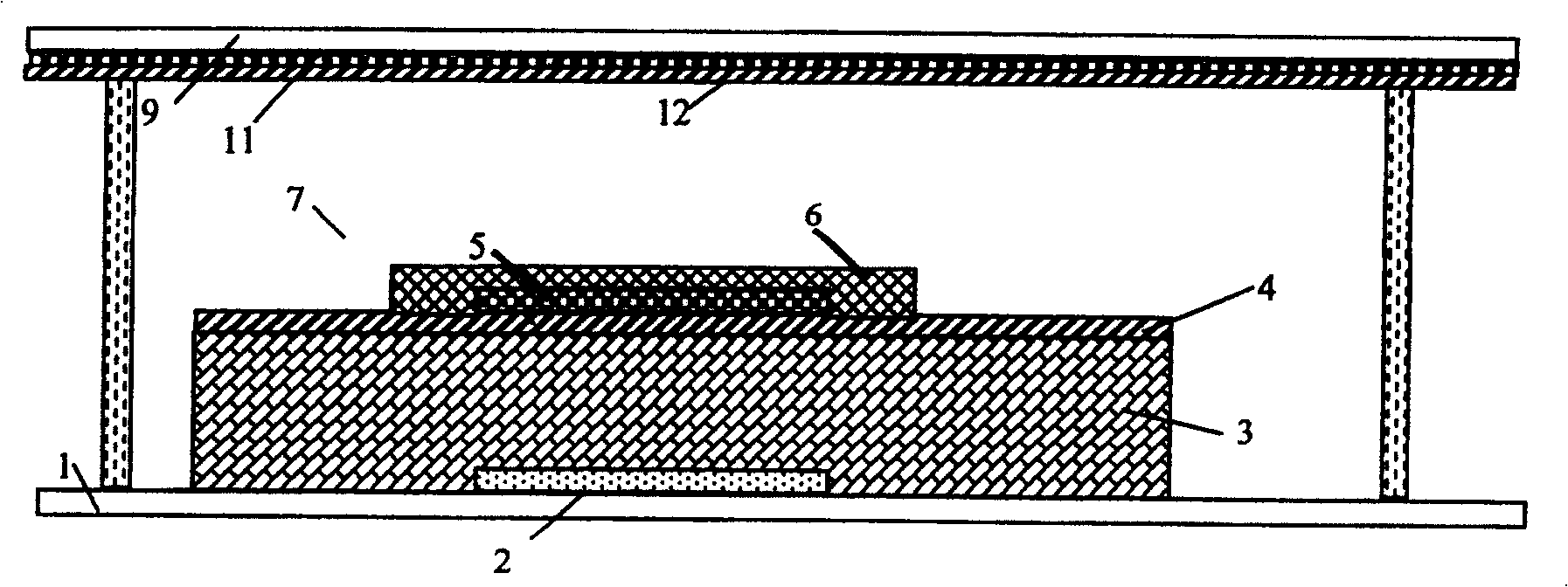
[0027] In the novel planar field emission triode structure of the present invention, a data electrode 2 is arranged on the cathode glass substrate 1, and a horizontal stripe-shaped dielectric layer 3 perpendicular thereto is arranged on the data electrode 2. The row scan electrode 4 is provided with a connection electrode 5 parallel to the data electrode 2 on the row scan electrode 4, and a field emission material 6 with a certain resistance characteristic is provided at the gap between the connection electrode 5 and the row scan electrode 4; A support body 7 is provided on the cathode glass substrate 1 or the dielectric layer 3, an anode glass substrate 8 is provided on the support body 7, an anode electrode 10 is provided on the lower surface of the anode glass substrate 8, and an anode electrode 10 is provided on the lower surface of the anode electrode 10. Phosphor layer 11.

[0028] The anode glass substrate 8 is made up of the transparent conductive film on the transpare...


PUM


Abstract

The method comprises: setting the data electrode on the glass cathode baseboard; on the data electrode, setting the dielectric layer with a horizontal bar shape and perpendicular with the data electrode; on the dielectric layer, setting the row scanning electrode; on the row scanning electrode, setting the connection electrode parallel with the data electrode; at the gap between the connection electrode and the row scanning electrode, setting a field emission material with a certain resistance property; on the glass cathode base board and the dielectric layer, setting the supporter; on the supporter, setting a anode glass baseboard; on the lower surface the glass anode baseboard, setting the anode electrode; on the lower surface of the anode electrode, setting a fluorescent powder layer.

Description

technical field [0001] The invention relates to a field emission display device and a manufacturing method, and relates to the design and preparation method of a triode structure in the field emission display device. Background technique [0002] At present, field emission display device (FED), as a new type of flat panel display device, still has a certain distance from marketization, and there are some key technical bottlenecks. Among them, the design and preparation of the triode structure is an important factor affecting the practical application of field emission display devices. [0003] The simplest field emission display can be formed by adopting a diode structure, and the display of video images can be realized through matrix scanning. In a field emission display with a two-pole structure, on the one hand, the anode needs high voltage to give electrons enough energy to bombard the phosphor to achieve high brightness; Therefore, there is a contradiction between the...

Claims


Application Information

Patent Timeline
Patent Type & Authority Patents(China)
IPC IPC(8): H05B33/02
Inventor 雷威张晓兵娄朝刚
Owner SOUTHEAST UNIV
Why Eureka
Try Eureka