Electrostatic-proof protection structure using NMOS

A technology for electrostatic protection and protection structure, which is applied to emergency protection circuit devices, emergency protection circuit devices, circuits and other directions for limiting overcurrent/overvoltage, which can solve the problem of different turn-on voltages and inability to fully exert ESD protection capabilities. The problem of low ESD protection ability of the tube can solve the problem of different turn-on voltages.

Active Publication Date: 2009-04-01
SHANGHAI HUAHONG GRACE SEMICON MFG CORP
View PDF4 Cites 1 Cited by
  • Summary
  • Abstract
  • Description
  • Claims
  • Application Information

AI Technical Summary

Problems solved by technology

[0003] The technical problem to be solved by the present invention is to provide an anti-static protection structure using NMOS, which can solve the ESD protection ability caused by the inability of the protection tube to uniformly conduct and discharge when the GGNMOS (Gate Ground NMOS grid-grounded NMOS) structure is used as ESD protection. not high problem
[0005] In the case of not changing the process conditions, by changing the connection mode of the parallel NMOS and adding NWELL injection in the drain region, the principle that the NMOS can be triggered at a low voltage effectively solves the problem that the turn-on voltage of the parallel NMOS protection device is not stable when ESD occurs. First, the problem that the ESD protection ability cannot be fully exerted

Method used


Image

  • Electrostatic-proof protection structure using NMOS
  • Electrostatic-proof protection structure using NMOS
  • Electrostatic-proof protection structure using NMOS

Examples


Embodiment Construction

[0012] The present invention will be described in further detail below in conjunction with the accompanying drawings and specific embodiments.

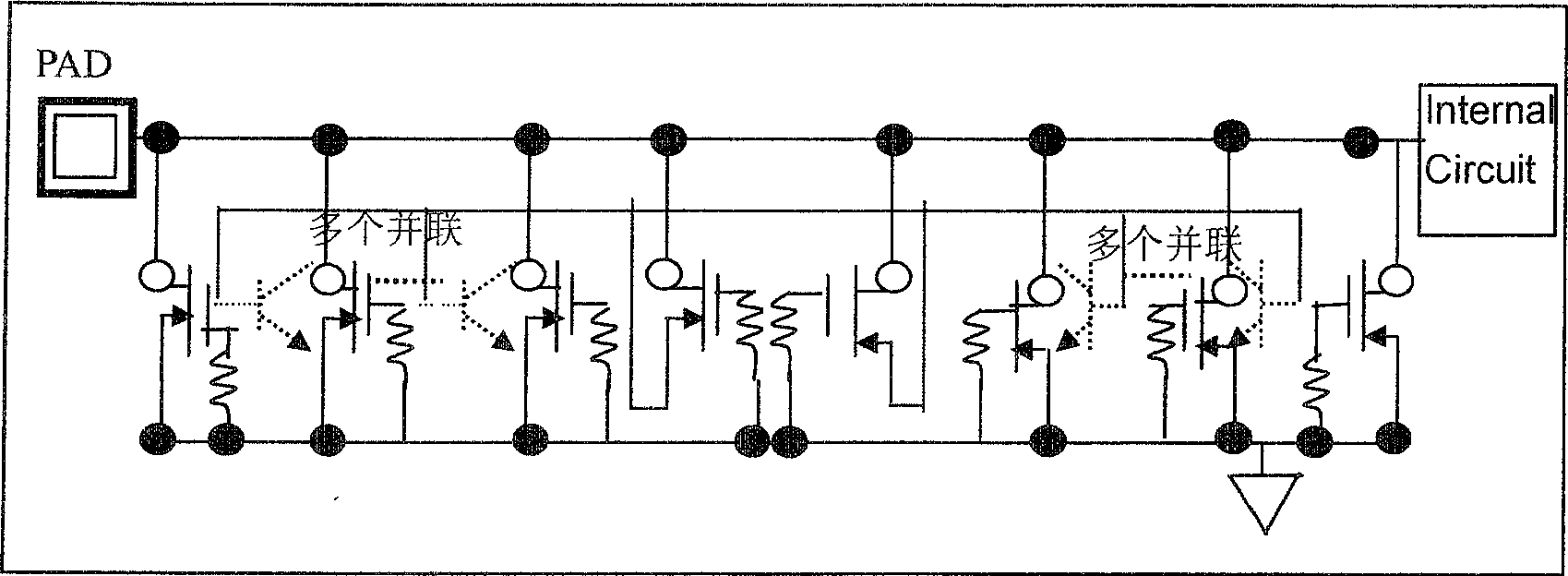
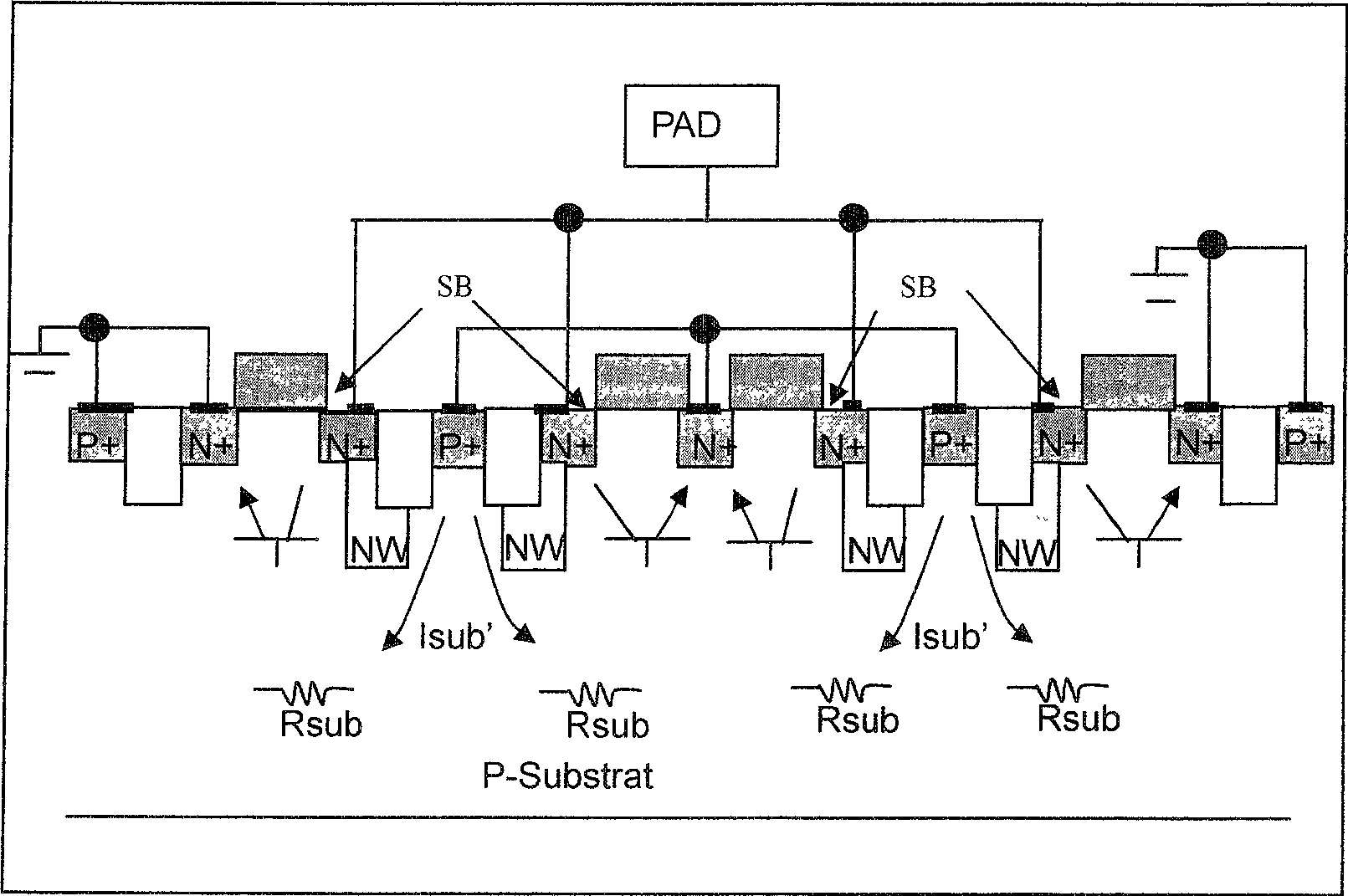
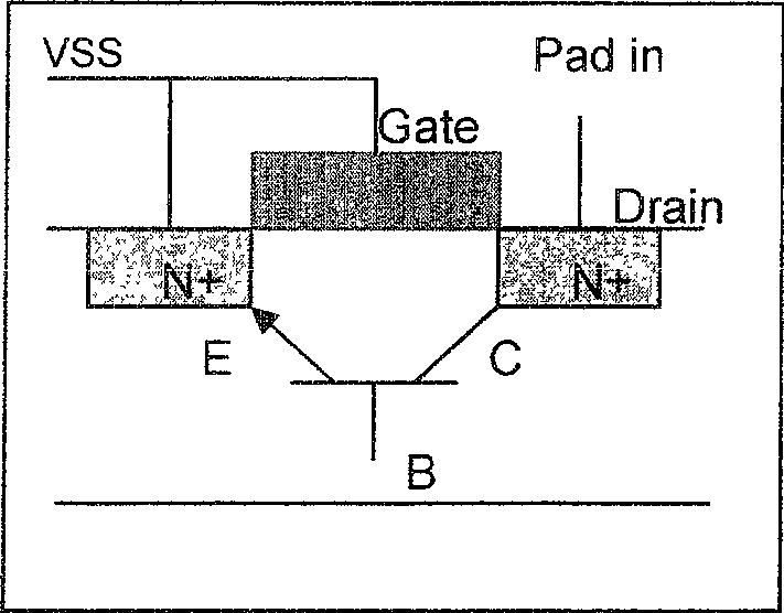
[0013] First set forth the inventive idea of ​​the present invention: firstly, explain the working state of GGNMOS when ESD occurs, because the base (substrate) and the PN junction of the emitter (source) of the NPN triode of NMOS parasitic should be in the positive state when effusion The direction is turned on, so the bias voltage applied to the base should be 0.7V higher than the emitter. This bias is related to the substrate current and the substrate resistance. Under the condition that the substrate current is constant, the greater the substrate resistance, the higher the base The larger the bias voltage on , the earlier the parasitic NPN can be turned on. However, experiments have proved that when ESD occurs, the NMOS parasitic NPN that is always in the center is turned on first, which may result in a low ESD protection capabili...


PUM


Abstract

In the invention, NMOS with grid being connected to ground is as basic part to constitute static protection circuit. Number of NMOS is even, and at least is four. Using N well at drain pole injects NWELL enhanced NMOS triggered at low voltage to drain area. Each NMOS is setup at centers of the static protection circuit, and their grid poles are connected to each other and their drain poles are connected to each other. Besides NMOS setup in centers, drain poles of NMOS at two sides are connected, and their source poles and grid poles are connected respectively in parallel. Source poles of NMOS in centers are connected to base pole of parasitic NPN of NMOS at two sides connected in parallel. When parasitic NPN of NMOS at centers are in on and effusion state, current is shunted to parasitic NPN of NMOS at two sides also so as to turn to on state between base pole and emitter of NMOS at two sides. The invention conducts effusion uniformly, and raises ESD protective power.

Description

technical field [0001] The invention relates to an antistatic circuit structure, in particular to an antistatic protection structure using NMOS. Background technique [0002] The current popular process technology uses CMOS (Complementary Metal-Oxide-Semiconductor Transistor) as an electrostatic discharge (ESD, ElectroStatic Discharge) protection device. When ESD occurs, the discharged electrostatic charge will cause the protection tube Nmos ( N-channel metal-oxide semiconductor, N-channel metal oxide semiconductor) parasitic triode conduction, such as image 3 As shown, the phenomenon of Snapback (that is, step recovery) will occur, such as Figure 4 ; Before entering the BC region of the normal effusion state, the protection tube needs to reach the opening voltage of point A. The turn-on voltage is determined by the substrate current and substrate resistance formed by the reverse leakage of the PN junction at the drain end. Because the circuit structure will cause the eff...

Claims


Application Information

Patent Timeline
Patent Type & Authority Patents(China)
IPC IPC(8): H01L23/60H02H9/00
Inventor 苏庆金锋徐向明
Owner SHANGHAI HUAHONG GRACE SEMICON MFG CORP
Why Eureka
Try Eureka