

Semiconductor device and its production method
A semiconductor and device technology, applied in the field of semiconductor devices of active matrix liquid crystal displays, can solve the problems of shortening heating time, reducing the accuracy of mask plate position and the like, and the like
- Summary
- Abstract
- Description
- Claims
- Application Information
AI Technical Summary
Problems solved by technology
Method used
Image

Examples
no. 1 Embodiment
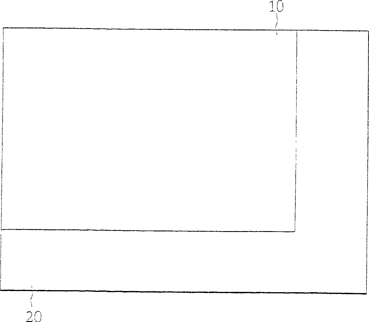
[0042] figure 1 It is a schematic top view diagram of the liquid crystal display structure of the embodiment of the present invention. The picture element part 10 shown in the figure has many picture element electrodes supplied in a matrix shape (not shown), and the peripheral circuit part 20 is used as driving each A drive circuit for the picture element electrodes. According to the present invention, thin film transistors (TFTs) for driving picture elements and peripheral circuits constituted by them are formed on an insulating substrate (ie, a glass substrate). Actually, the peripheral circuit part is constituted as a CMOS circuit in which a P-channel type TFT s (PTFT) and N-channel TFT s (NTFT) is composed of a silicon film (called a single crystal film) with a crystallized growth in the lateral direction, and the image element part is a TFT composed of an amorphous silicon film as NTFT s .
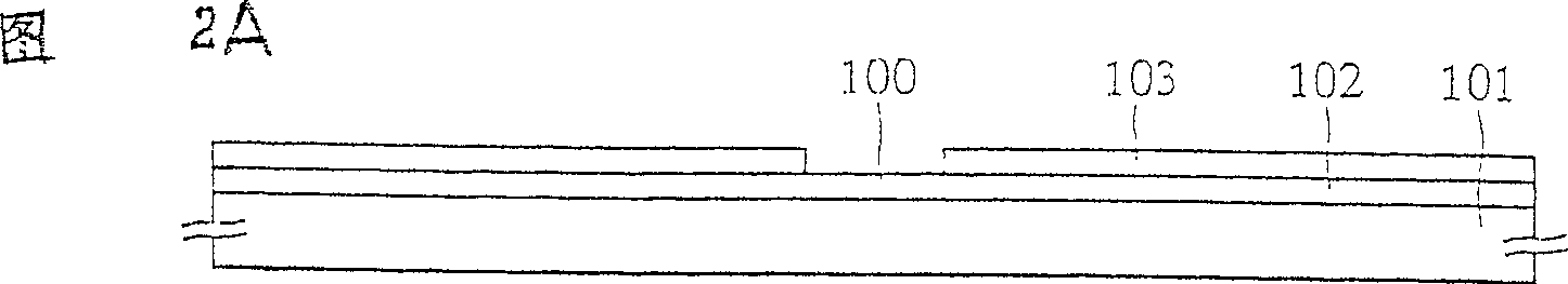
[0043] 2A to 2D are diagrams showing a circuit manufacturing process in which...
no. 2 Embodiment
[0065] The second embodiment is shown in FIGS. 5A to 5E and FIGS. 6A and 6B. After forming a silicon oxide film 502 with a thickness of 1000 to 5000 angstroms, such as 2000 angstroms, on the surface of the glass substrate 501, form an amorphous silicon film with a thickness of 300 to 1500 angstroms, such as 500 angstroms, on it by plasma CVD, and then , and then form a silicon oxide film 504 with a thickness of 500 to 1500 angstroms, for example, 500 angstroms. It is preferable to form these films continuously. Then, the silicon oxide film 50A is selectively etched to form a window region 506 into which nickel is introduced. In the manufacture of TFTs used as peripheral circuits s The window area 506 is formed in the area, and the window area 506 is not formed in the picture element portion.
[0066] Next, a nickel salt thin film 505 is formed by spin coating. Next, the spin coating method will be explained. First, nickel acetate or nickel nitrate is diluted with water or...
PUM
| Property | Measurement | Unit |
|---|---|---|
| thickness | aaaaa | aaaaa |
| thickness | aaaaa | aaaaa |
| thickness | aaaaa | aaaaa |
Abstract
Description
Claims
Application Information