Imaging box chip as well as read-write method, imaging box and imaging device thereof

A technology of imaging box chip and reading and writing method, which is applied in the field of imaging, can solve the problems of difficult chip data modification, no proper solution is proposed, and the flexibility of imaging box chip is reduced, so as to achieve the effect of reducing the implementation cost

Inactive Publication Date: 2010-07-21
ZHUHAI SEINE TECH CO LTD
View PDF0 Cites 26 Cited by
  • Summary
  • Abstract
  • Description
  • Claims
  • Application Information

AI Technical Summary

Problems solved by technology

[0004] However, during the research process of the present invention, the inventor found that the prior art has the following defects: the imaging box chip uses a storage unit to pre-store matching information. O

Method used


Image

  • Imaging box chip as well as read-write method, imaging box and imaging device thereof
  • Imaging box chip as well as read-write method, imaging box and imaging device thereof
  • Imaging box chip as well as read-write method, imaging box and imaging device thereof

Examples


Embodiment 1

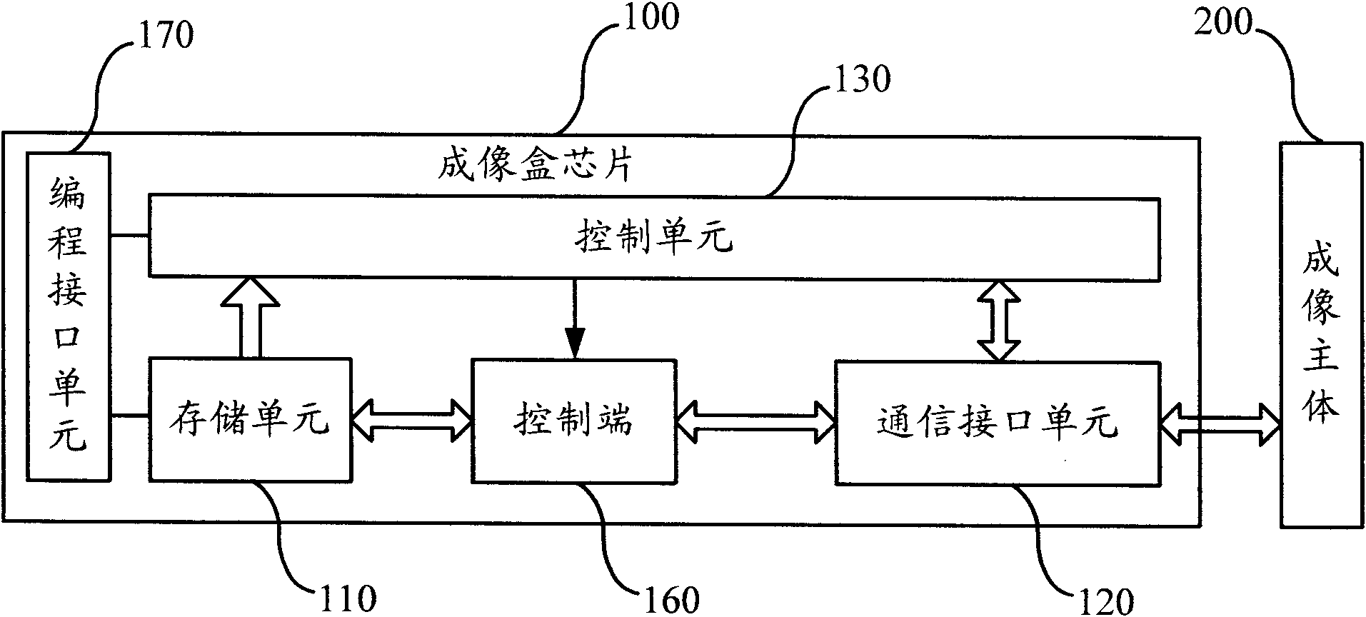
[0046] figure 1 It is a schematic structural diagram of the imaging cartridge chip provided by Embodiment 1 of the present invention. The imaging box chip 100 includes a storage unit 110 , a communication interface unit 120 and a control unit 130 . The storage unit 110 is used to store relevant information of the imaging cartridge, such as printing information and matching information provided to the imaging subject 200 for matching and identification. The password used, etc. The communication interface unit 120 provides an interactive interface between the storage unit 110 and the imaging subject 200 , receives read and write instructions sent by the imaging subject 200 and outputs a response returned by the imaging cartridge chip 100 . The control unit 130 is connected with the communication interface unit 120, and is used to obtain the setting matching information according to the pre-stored information of the control unit 130 and return it to the imaging subject when it ...

Embodiment 2

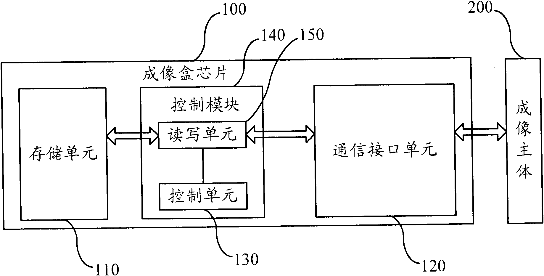
[0052] image 3 It is a schematic structural diagram of the imaging cartridge chip provided by Embodiment 2 of the present invention. In this embodiment, the control unit 130 is arranged in the control module 140 and is connected to the read-write unit 150 in the control module 140, that is, indirectly connected to the communication interface unit 120; the read-write unit 150 is arranged in the storage unit 110 and the communication interface unit 120 In between, it is used to receive the read and write instructions sent by the imaging subject 200 to control the read and write operations of the imaging subject 200 in the storage unit 110 .

[0053] The control module 140 may be an original control component in the imaging cartridge chip 100, and the control unit 130 may be integrated in the control module 140 in the form of software or hardware. When the control unit 130 provides the setting matching information, the read-write unit 150 may be controlled to cut off the commun...

Embodiment 3

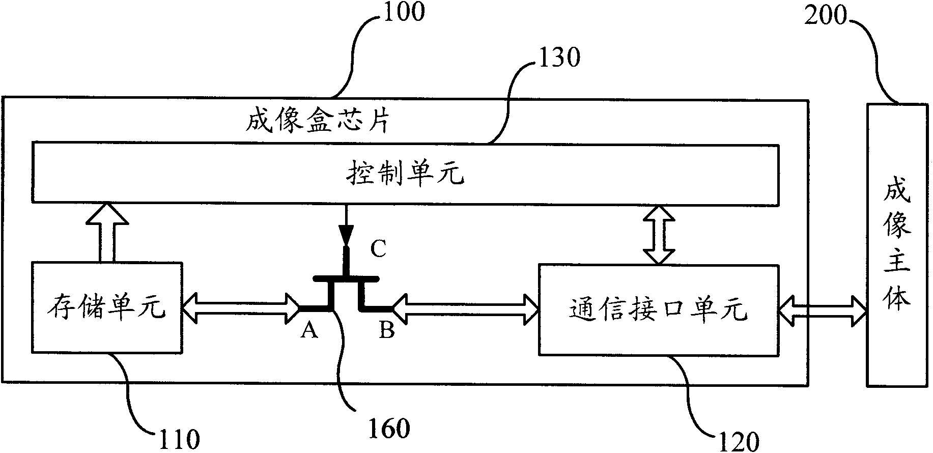
[0056] Figure 4 It is a schematic structural diagram of the imaging cartridge chip provided by Embodiment 3 of the present invention. This embodiment is based on the first or second embodiment above, and the control unit 130 specifically includes: an identification subunit 131 and a return subunit 132 . Wherein, the identification subunit 131 is connected with the communication interface unit 120, and is used to intercept the read and write instructions of the imaging subject 200 to read and write data in the storage unit 110, and when the read address in the read and write instructions is consistent with the pre-stored set address, Or when the identifier in the read-write instruction is consistent with the pre-stored identifier, it is determined that the read-write instruction is an instruction for reading setting matching information; the return subunit 132 is connected with the identification subunit 131, and is used for when the identification subunit 131 resolves to read...


PUM


Abstract

The invention discloses an imaging box chip as well as a read-write method, an imaging box and an imaging device thereof. The imaging box chip comprises a storage unit, a communication interface unit and a control unit. The control unit is connected with the communication interface unit and is used for obtaining set matching information and returning the set matching information to an imaging body according to the prestored information of the control unit when the imaging body is analyzed to read an instruction of the set matching information from the storage unit, so that the matching identification is carried out. In the technical scheme, the control unit provides the imaging body with the preset matching information when the imaging body needs to read the set matching information for identification, so that the imaging body identifies the imaging box and the imaging box passes the verification for carrying out imaging operation. The technical scheme provides an executing scheme when the matching information in the storage unit needs to be modified so as to provide modified matching information, avoid developing chips repeatedly and reduce the development cost of the chip.

Description

technical field [0001] Embodiments of the present invention relate to imaging technology, and in particular to an imaging box chip, a reading and writing method thereof, an imaging box, and an imaging device. Background technique [0002] The imaging device generally includes an imaging main body and an imaging box, and the imaging box is detachably installed on the imaging main body. Image forming devices come in various forms, such as printers, copiers, and scanners. Imaging cartridges, such as ink cartridges, toner cartridges, etc., are loaded with recording materials for imaging, and the imaging subject uses the imaging cartridges to form images on paper and other media. Generally, a storage chip is fixedly arranged on the imaging box, which may be referred to as an imaging box chip. The imaging cartridge chip generally includes a storage unit and a communication interface unit. The storage unit not only records the relevant information of the imaging cartridge, such a...

Claims


Application Information

Patent Timeline
IPC IPC(8): G03G21/18G03G15/08B41J2/175
Inventor 宋丰君祁美超楼鹏
Owner ZHUHAI SEINE TECH CO LTD
Why Eureka
Try Eureka