Misfit-layered cobalt oxide pyroelectric thin-film photodetector

A pyroelectric film and photodetector technology, which is applied in the field of high-sensitivity broadband photodetectors, can solve the problems of not seeing photodetectors, and achieve the effects of high response sensitivity, low cost, and fast response time

Inactive Publication Date: 2010-09-08
HEBEI UNIVERSITY
View PDF1 Cites 18 Cited by
  • Summary
  • Abstract
  • Description
  • Claims
  • Application Information

AI Technical Summary

Problems solved by technology

But so far, there is no report on the preparation of

Method used


Image

  • Misfit-layered cobalt oxide pyroelectric thin-film photodetector
  • Misfit-layered cobalt oxide pyroelectric thin-film photodetector
  • Misfit-layered cobalt oxide pyroelectric thin-film photodetector

Examples


Embodiment 1

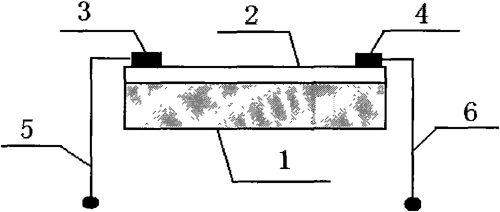
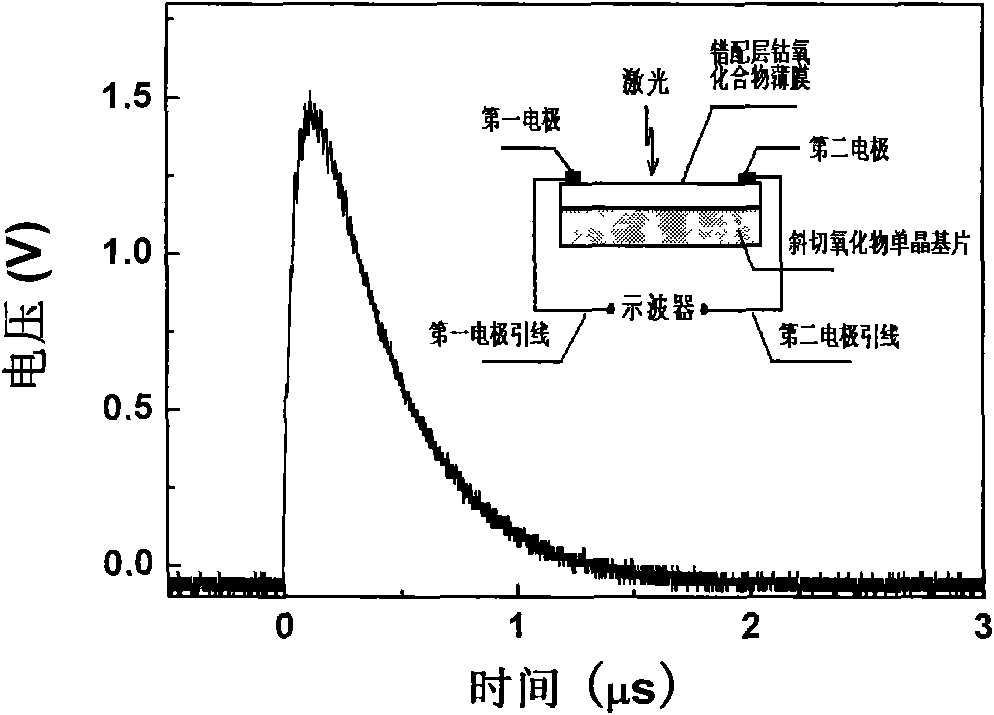
[0024] Embodiment 1: the Bi that can output laser detection to the 308nm XeCl excimer laser with a pulse width of 25ns 2 Sr 2 co 2 o 8 Thin-film photodetectors.

[0025] 1. Select the known pulsed laser deposition technology in the c-axis orientation LaAlO tilted at 10 degrees 3 Preparation of a layer of c-axis-oriented Bi with a thickness of 200 nm on a single crystal substrate 2 Sr 2 co 2 o 8 Thermoelectric thin film;

[0026] 2. Utilizing known thermal evaporation methods in Bi 2 Sr 2 co 2 o 8 Prepare two Ag electrodes on the surface of the film, the diameter of the electrodes is 0.5mm, and the distance between the electrodes is 5mm;

[0027] 3. Use conductive silver glue to stick two copper wires with a diameter of 0.1mm on the two silver electrodes respectively as the leads of the two electrodes;

[0028] 4. Connect the other ends of the two electrode leads to the oscilloscope as the output voltage signal test terminal, and the input impedance of the oscillos...

Embodiment 2

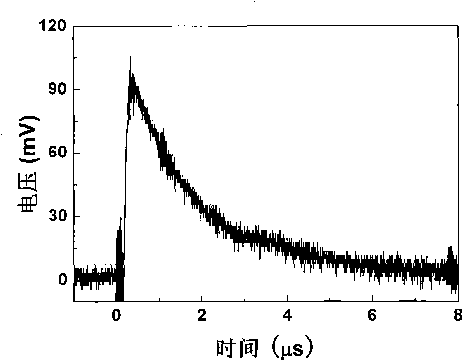
[0031] Example 2: Ca that can be detected by a 308nm XeCl excimer laser with a pulse width of 25ns 3 co 4 o 9 Thin-film photodetectors.

[0032] 1. Select the known chemical solution deposition technology at 20 degrees inclined c-axis orientation of Al 2 o 3 A layer of c-axis-oriented Ca with a thickness of 300 nm was prepared on a single crystal substrate 3 co 4 o 9 Thermoelectric thin film;

[0033] 2. With step 2-4 in embodiment 1;

[0034] 5. Use a 500M oscilloscope, use the above Ca 3 co 4 o 9 Thin-film photodetector, measuring the voltage signal output of the excimer XeCl laser (output wavelength: 308nm, pulse width: 25ns) irradiated on the detector.

[0035] image 3 It is the waveform diagram of the output voltage signal generated when the 308nm XeCl laser is irradiated on the surface of the detector recorded by the oscilloscope. It can be seen that when the laser energy irradiated on the thin film is 1mJ, the amplitude of the output voltage signal is as hig...

Embodiment 3

[0036] Embodiment 3: the Bi that can be detected by the Nd:YAG laser output laser (output wavelength is 532nm) to the pulse width of 25ps 2 Sr 2 co 2 o 8 Thin-film photodetectors.

[0037] 1. Select the known chemical solution deposition technology at 5 degrees inclined c-axis orientation of LaAlO 3 Preparation of a layer of c-axis-oriented Bi with a thickness of 150 nm on a single crystal substrate 2 Sr 2 co 2 o 8 Thermoelectric thin film;

[0038] 2. Prepare two In electrodes on the surface of the film by using a known thermal evaporation method, the diameter of the electrodes is 0.3mm, and the distance between the electrodes is 8mm;

[0039] 3. Use solder to weld two copper wires with a diameter of 0.1mm on the two In electrodes respectively as the leads of the two electrodes;

[0040] 4. Connect the other ends of the two electrode leads to the oscilloscope as the output voltage signal test terminal, and the input impedance of the oscilloscope is selected as 50 ohm...


PUM

PropertyMeasurementUnit
Membrane thicknessaaaaaaaaaa
Diameteraaaaaaaaaa
Resistanceaaaaaaaaaa

Abstract

The invention provides a misfit-layered cobalt oxide pyroelectric thin-film photodetector, belongs to the technical field of thin-film photodetector equipment, and solves the technical problem of providing the photodetector which is manufactured by growing a layer of c-axially oriented misfit-layered cobalt oxide pyroelectric thin-film on a beveled oxide monocrystal substrate. The photodetector comprises a technical scheme that the photodetector consists of the beveled oxide monocrystal substrate and the c-axially oriented misfit-layered cobalt oxide pyroelectric thin-film, wherein the c-axially oriented misfit-layered cobalt oxide pyroelectric thin-film grows on the beveled oxide monocrystal substrate by adopting pulsed laser deposition technology or metal organic deposition technology; the thin-film surface is provided with two electrodes which are deposited on the thin-film surface by using thermal evaporation, magnetron sputtering or pulsed laser deposition technology; and the two electrodes are connected with an output end of a voltage signal through electrode lead wires respectively. The misfit-layered cobalt oxide pyroelectric thin-film photodetector provided by the invention has the advantages of simple preparation, low cost, wide response wave band, high response sensitivity and quick response.

Description

technical field [0001] The invention relates to a high-sensitivity wide-band photodetector made by using a cobalt oxide compound thermoelectric thin film of a mismatch layer, and belongs to the technical field of thin-film photodetector equipment. Background technique [0002] When a laser beam is irradiated on the surface of a thin film deposited on an inclined single crystal substrate, a temperature difference will be generated between the upper and lower surfaces of the thin film, and a temperature difference will be generated at both ends of the thin film due to the anisotropy of the Seebeck coefficient of the thin film. The transverse voltage signal and the amplitude of the voltage signal are proportional to the difference ΔS of the Seebeck coefficient in the ab-axis direction and the c-axis direction of the thin film material. This effect is called the laser-induced thermal voltage effect. In recent years, new photodetectors fabricated using the laser-induced thermal v...

Claims


Application Information

Patent Timeline
IPC IPC(8): H01L35/28H01L35/22
Inventor 王淑芳陈景春傅广生陈明敬何立平于威李晓苇
Owner HEBEI UNIVERSITY
Why Eureka
Try Eureka