Optical delayer coupled through adopting multiple-mode interference

A multi-mode interference and delay device technology, applied in the field of optical buffering, can solve the problems of difficult device acquisition and large working bandwidth, and achieve the effects of high repeatability, large working bandwidth and easy production.

Inactive Publication Date: 2010-11-10
INST OF MICROELECTRONICS CHINESE ACAD OF SCI
View PDF0 Cites 13 Cited by
  • Summary
  • Abstract
  • Description
  • Claims
  • Application Information

AI Technical Summary

Problems solved by technology

[0006] The purpose of the present invention is to solve the problem that the evanescent field coupling method of the slit structure in the optical delay device of the silicon-based microring cascade structure is difficult to obtain a large operating bandwidth for the device, and provides a multi-mode interference coupling Wide Bandwidth Optical Delay

Method used


Image

  • Optical delayer coupled through adopting multiple-mode interference
  • Optical delayer coupled through adopting multiple-mode interference
  • Optical delayer coupled through adopting multiple-mode interference

Examples


Embodiment Construction

[0024] In order to make the object, technical solution and advantages of the present invention clearer, the present invention will be described in further detail below in conjunction with specific embodiments and with reference to the accompanying drawings.

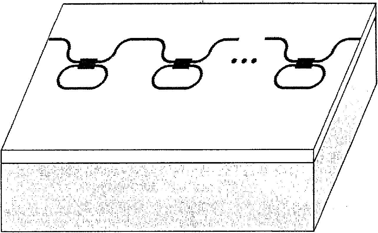
[0025] figure 1 Shown is a schematic structural diagram of an optical delayer using multi-mode interference coupling provided by the present invention. The optical delayer adopts an all-pass filter structure, which is a structure in which several microring resonators are sequentially coupled to the bus waveguide, and the coupling section between the microring resonator and the bus waveguide is 2×2 Multimode interference coupler.

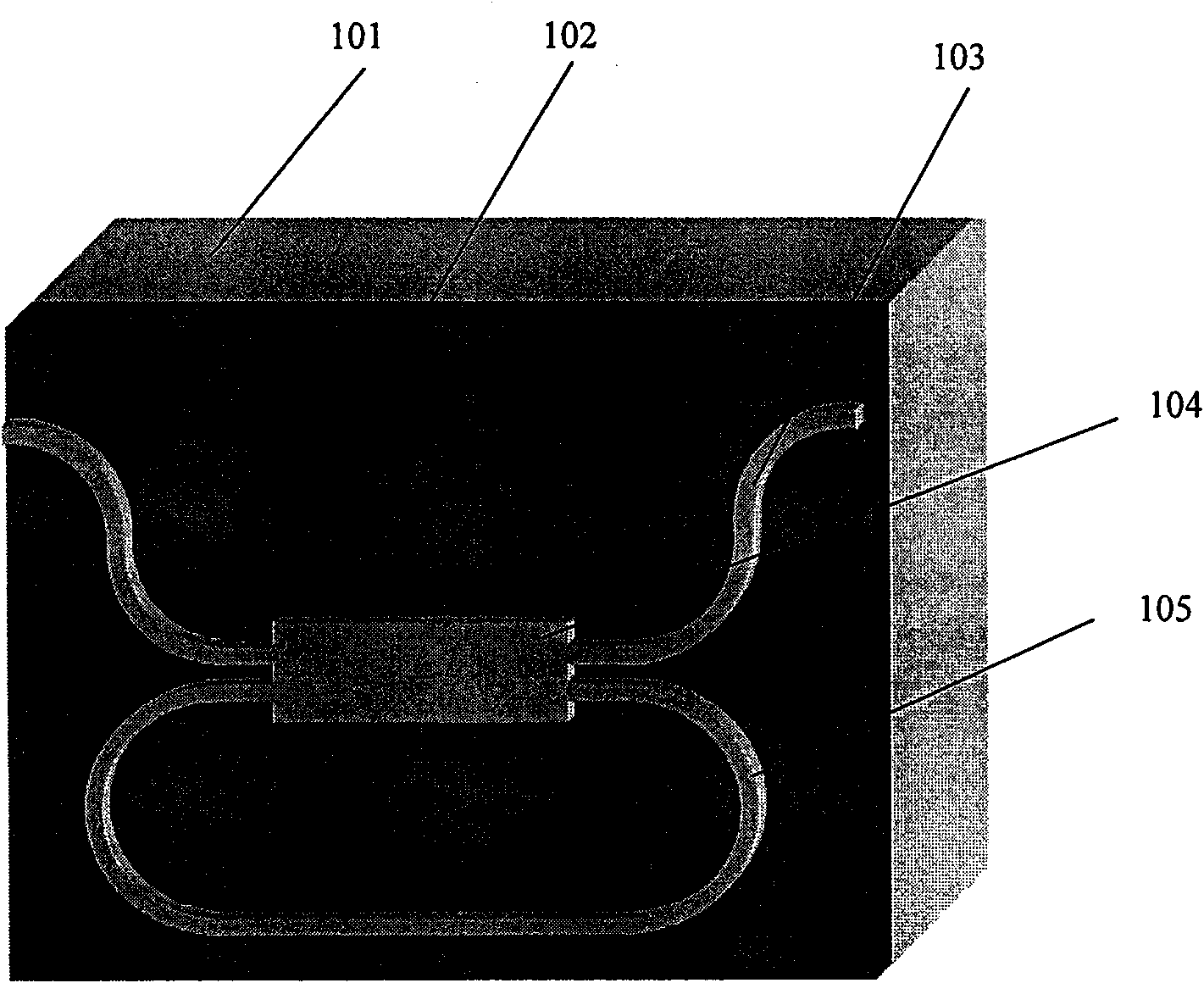
[0026] figure 2 Shown is a three-dimensional schematic diagram of the basic structural unit of the new optical delayer using multi-mode interference coupling. The optical delay device is manufactured based on an SOI substrate 101, the BOX (buried oxide layer) layer 102 is silicon oxide with ...


PUM


Abstract

The invention discloses an optical delayer coupled through adopting multiple-mode interference, which adopts an all-pass filter structure; the all-pass filter structure is a structure of the sequent coupling of a plurality of micro ring resonant cavities and a bus waveguide, wherein the coupled segment between the micro ring resonant cavities and the bus waveguide is of a 2*2 multiple-mode interference coupler. Adopting the multiple-mode interference coupled structure, the invention can improve the coupling efficiency between the micro ring resonant cavities and the bus waveguide, and makes the optical delayer have wider operation bandwidth. The invention has high technical redundancy, is easy to manufacture, has small size, is suitable for dense integration, also has the characteristics of wide bandwidth and big time delay, the structural design with different splitting ratio increases the flexibility of the device application, and the delayer is suitable for being used as an optical buffer device of high-speed all-optical packet switching network in the future.

Description

technical field [0001] The invention relates to the technical field of optical buffering of an all-optical packet switching network, in particular to an optical delayer adopting multi-mode interference coupling. Background technique [0002] Optical buffering technology is an essential part of all-optical packet switching network. In the optical switching of network nodes, optical buffering is responsible for resolving conflicts and is the basic device for realizing optical-optical switching. The optical delay line is the most common optical buffer device, and its function is to extend the propagation path of light and generate optical delay. With the rapid increase of the speed and capacity of optical network information transmission, it is required that the optical delay device should have the characteristics of large delay, small size and large working bandwidth. Silicon-on-insulator (SOI) material is an excellent platform for monolithic photonic integration. The high re...

Claims


Application Information

Patent Timeline
Patent Type & Authority Applications(China)
IPC IPC(8): G02B6/26
Inventor 周静涛申华军张慧慧刘新宇
Owner INST OF MICROELECTRONICS CHINESE ACAD OF SCI
Why Eureka
Try Eureka